Samsung's s5p6818 FULL device tree decortication (kernel4.4)
This is a full device-tree decoritcation of Samsung’s S5p6818 SoC in addition to the device tree of the gec-lab’s board GEC6818.
####################################################################################################################################
#### SoC DTS
####################################################################################################################################
/*
* Copyright (C) 2016 (kernel4.4) Nexell Co., Ltd.
* Author: Youngbok, Park <ybpark@nexell.co.kr>
*
* This program is free software; you can redistribute it and/or
* modify it under the terms of the GNU General Public License
* as published by the Free Software Foundation; either version 2
* of the License, or (at your option) any later version.
*
* This program is distributed in the hope that it will be useful,
* but WITHOUT ANY WARRANTY; without even the implied warranty of
* MERCHANTABILITY or FITNESS FOR A PARTICULAR PURPOSE. See the
* GNU General Public License for more details.
*
* You should have received a copy of the GNU General Public License
* along with this program. If not, see <http://www.gnu.org/licenses/>.
*/
#include <dt-bindings/tieoff/s5p6818-tieoff.h>
#include <dt-bindings/soc/s5p6818-base.h>
#include <dt-bindings/reset/nexell,s5p6818-reset.h>
#include <dt-bindings/interrupt-controller/s5p6818-irq.h>
#include <dt-bindings/media/nexell-vip.h>
/ {
model = "nexell soc";
compatible = "nexell,s5p6818";
#address-cells = <0x1>;
#size-cells = <0x1>;
A devicetree may have an aliases node (/aliases) that defines one or more alias properties. The alias node shall be at the root of the devicetree and have the node name /aliases.
Alias names shall be a lowercase text strings of 1 to 31 characters from the following set of characters: 0-9 a-z and dash -
The main usage of the alias node is that a client program may use an alias property name to refer to a full device path, instead of looking for it in the full tree.
aliases {
serial0 = &serial0;
serial1 = &serial1;
serial2 = &serial2;
serial3 = &serial3;
serial4 = &serial4;
serial5 = &serial5;
i2s0 = &i2s_0;
i2s1 = &i2s_1;
i2s2 = &i2s_2;
spi0 = &spi_0;
spi1 = &spi_1;
spi2 = &spi_2;
i2c0 = &i2c_0;
i2c1 = &i2c_1;
i2c2 = &i2c_2;
pinctrl0 = &pinctrl_0;
};
Power State Coordination Interface (PSCI):
It defines a standard interface for power management that can be used by operating system vendors, for supervisory software working at different levels of privilege on an Arm device.
Rich operating systems, like Linux and Windows, use PSCI for CPU and overall system power management. The interface covers the following scenarios:
- Core idle management.
- Dynamic addition and removal of cores, and secondary core boot.
- System shutdown and reset.
The interface does not cover Dynamic Voltage and Frequency Scaling (DVFS) or device power management (for example, management of peripherals, such as GPUs). System Control and Management Interface (SCMI) does provide standard interfaces for this purpose.
The interface is designed so that it can work in conjunction with hardware discovery technologies, such as Advanced Configuration and Power Interface and Flattened Device Tree. psci.txt
Firmware implementing the PSCI functions described in ARM document number ARM DEN 0022A ("Power State Coordination Interface System Software on ARM processors") can be used by Linux to initiate various CPU-centric power operations.
Issue A of the specification describes functions for CPU suspend, hotplug and migration of secure software.
Functions are invoked by trapping to the privilege level of the PSCI firmware (specified as part of the binding below) and passing arguments in a manner similar to that specified by AAPCS:
r0 => 32-bit Function ID / return value
{r1 - r3} => Parameters
Note that the immediate field of the trapping instruction must be set to #0.
psci {
compatible = "arm,psci-0.2"; Function IDs are not required and should be ignored by an OS with PSCI 0.2 support
method = "smc"; The method of calling the PSCI firmware. in this case : smc #0 (not hvc)
};
A memory device node is required for all devicetrees and describes the physical memory layout for the system. If a system has multiple ranges of memory, multiple memory nodes can be created, or the ranges can be specified in the reg property of a single memory node. The unit-name component of the node name (see section 2.2.1) shall be memory.
memory {
device_type = "memory";
reg = <0x40000000 0x7db00000>; an arbitrary number of address and size pairs that specify the physical address and size of the memory ranges.
};
The operating system shall exclude reserved memory from normal usage. One can create child nodes describing particular reserved (excluded from normal use) memory regions. Such memory regions are usually designed for the special usage by various device drivers.
reserved-memory {
#address-cells = <1>;
#size-cells = <1>;
The ranges property provides a means of defining a mapping between the address space of the bus and that of the bus node’s parent
If the property is defined with an <empty> value, it specifies that the parent and child address space is identical. i.e., no translation is needed to be done for the child's reg addresses.
ranges;
};
cpus {
The #address-cells and #size-cells properties may be used in any device node that has children in the devicetree hierarchy and describes how child device nodes should be addressed. The #address-cells property defines the number of cells used to encode the address field in a child node’s reg property.
- The #size-cells property defines the number of cells used to encode the size field in a child node’s reg property.
- The #address-cells and #size-cells properties are not inherited from ancestors in the devicetree. They shall be explicitly defined.
- A DTSpec-compliant boot program shall supply #address-cells and #size-cells on all nodes that have children. If missing, a client program should assume a default value of 2 for #address-cells, and a value of 1 for #size-cells
#address-cells = <0x2>;
#size-cells = <0x0>;
cpu0: cpu@0 {
device_type = "cpu";
compatible = "arm,cortex-a53";
reg = <0x0 0x0>; this defines two threads per CPU with the second thread having the unique ID of the CPU core.
enable-method = "psci"; Describes the method by which a CPU in a disabled state is enabled.
cpu-release-addr = < 0x1 0xc0010230 >; On ARM v8 64-bit systems must be a two cell property identifying a 64-bit zero-initialised memory
location.
#cooling-cells = <2>;Used to provide cooling device specific information while referring to it. As this is defined in a CPU node, the cooling is
passive i.e., using DVFS…
Must be at least 2, in order to specify minimum and maximum cooling states used in the reference. These states have one-to-one correspondence with the operating points of the CPU i.e., if 5 OPPs are defined, the min cooling state will be 0 and max will be 4.
NEXELL SPECIFIC : This property is defined without defining any operating-points for the CPU !!!!!!!!!!!!!!!!!!!!!!!!!!!!!!!
Well, it turned out that 13 operating points are defined in drivers/cpufreq/s5p6818-cpufreq.h ASV table (which stands for Adaptive Supply Voltage). But you may ask why did they do that, why not simply use the operating-points standard device tree property. From the code, it is clear now that different operating points are available depending on the S5p6818 silicon revision. A dynamic way was needed for defining these operating points. In the code they check the SoC ID before setting the OPPs.
For more info regarding thermal management in dt see : Thermal Framework Device Tree descriptor in board DTS further below.
cpu-idle-states =<&CPU_SLEEP>; List of phandles to idle state nodes supported by this CPU.
ARM systems contain HW capable of managing power consumption dynamically, where cores can be put in different low-power states (ranging from simple WFI-Wait For Interrupt- to power gating) according to OS PM policies. The CPU states representing the range of dynamic idle states that a processor can enter at run-time, can be specified through device tree bindings representing the parameters required to enter/exit specific idle states on a given processor. idle-states.txt
};
cpu1: cpu@1 {
device_type = "cpu";
compatible = "arm,cortex-a53";
reg = <0x0 0x1>;
enable-method = "psci";
cpu-release-addr = < 0x1 0xc0010230 >;
cpu-idle-states =<&CPU_SLEEP>;
};
cpu2: cpu@2 {
device_type = "cpu";
compatible = "arm,cortex-a53";
reg = <0x0 0x2>;
enable-method = "psci";
cpu-release-addr = < 0x1 0xc0010230 >;
cpu-idle-states =<&CPU_SLEEP>;
};
cpu3: cpu@3 {
device_type = "cpu";
compatible = "arm,cortex-a53";
reg = <0x0 0x3>;
enable-method = "psci";
cpu-release-addr = < 0x1 0xc0010230 >;
cpu-idle-states =<&CPU_SLEEP>;
};
cpu4: cpu@4 {
device_type = "cpu";
compatible = "arm,cortex-a53";
reg = <0x0 0x100>;
enable-method = "psci";
cpu-release-addr = < 0x1 0xc0010230 >;
cpu-idle-states =<&CPU_SLEEP>;
};
cpu5: cpu@5 {
device_type = "cpu";
compatible = "arm,cortex-a53";
reg = <0x0 0x101>;
enable-method = "psci";
cpu-release-addr = < 0x1 0xc0010230 >;
cpu-idle-states =<&CPU_SLEEP>;
};
cpu6: cpu@6 {
device_type = "cpu";
compatible = "arm,cortex-a53";
reg = <0x0 0x102>;
enable-method = "psci";
cpu-release-addr = < 0x1 0xc0010230 >;
cpu-idle-states =<&CPU_SLEEP>;
};
cpu7: cpu@7 {
device_type = "cpu";
compatible = "arm,cortex-a53";
reg = <0x0 0x103>;
enable-method = "psci";
cpu-release-addr = < 0x1 0xc0010230 >;
cpu-idle-states =<&CPU_SLEEP>;
};
ARM topology bindings allow one to associate cpu nodes with hierarchical groups corresponding to the system hierarchy. the hierarchy of CPUs is defined through three entities that are used to describe the layout of physical CPUs in the system: - cluster- core- thread
“thread“ nodes are defined only on systems where SMT (Symmetric MultiThreading) is not supported i.e. not directly covered by the core.
cpu-map {
cluster0 {
core0 {
cpu = <&cpu0>;
};
core1 {
cpu = <&cpu1>;
};
core2 {
cpu = <&cpu2>;
};
core3 {
cpu = <&cpu3>;
};
};
cluster1 {
core0 {
cpu = <&cpu4>;
};
core1 {
cpu = <&cpu5>;
};
core2 {
cpu = <&cpu6>;
};
core3 {
cpu = <&cpu7>;
};
};
};
idle-states {
Only one Idle state is define for all the CPUs: which is sleep
The idle state entered by executing the wfi instruction (idle_standby SBSA,[3][4]) is considered standard on all ARM platforms and therefore must not be listed here.
The following diagram depicts the CPU execution phases and related timing
properties required to enter and exit an idle state:
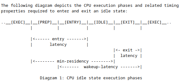
CPU_SLEEP: sleep {
compatible = "nexell,idle-state";
arm,psci-suspend-param = <0x0000000>; power_state parameter to pass to the PSCI suspend call. see psci node.
entry-latency-us = <150>; u32 value representing worst case latency in microseconds required to enter the idle state
exit-latency-us = <200>;u32 value representing worst case latency in microseconds required to exit the idle state.
The exit-latency-us duration may be guaranteed only after entry-latency-us has passed.
min-residency-us = <2000>; value representing minimum residency duration in microseconds, inclusive of preparation and entry
};
};
};
ARM Performance Monitor Units:
The Cortex-A53 processor includes performance monitors that implement the Arm PMUv3 architecture. These enable you to gather various statistics on the operation of the processor and its memory system during runtime. These provide useful information about the behavior of the processor that you can use when debugging or profiling code. The PMU provides six counters. Each counter can count any of the events available in the processor.
https://www.kernel.org/doc/Documentation/devicetree/bindings/arm/pmu.txt
pmu {
compatible = "arm,armv8-pmuv3"; could be also “arm,cortex-a53-pmu”
INTERRUPTS:
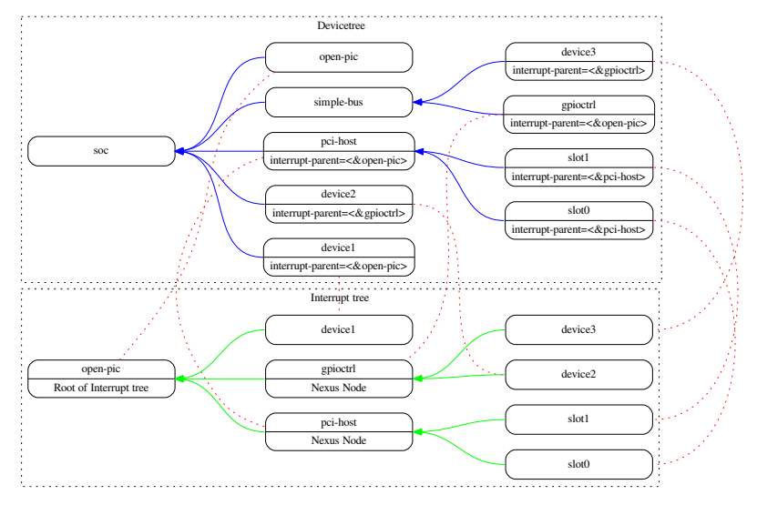
The physical wiring of an interrupt source to an interrupt controller is represented in the devicetree with the interrupt parent property. Nodes that represent interrupt-generating devices contain an interrupt-parent property which has a phandle value that points to the device to which the device’s interrupts are routed, typically an interrupt controller.
Each interrupt generating device contains an interrupts property with a value describing one or more interrupt sources for that device. Each source is represented with information called an interrupt specifier.
The #interrupt-cells property is used by the root (i.e., almost always the interrupt controller) of an interrupt domain to define the number of values needed to encode an interrupt specifier.
An interrupt controller is a physical device and will need a driver to handle interrupts routed through it. It may also cascade into another interrupt domain.
An interrupt controller is specified by the presence of an interrupt-controller property on that node in the devicetree.
interrupt-parent = <&gic>; define gic (generic interrupt controller) as the parent interrupt handler of the PMU.
The interrupts property of a device node defines the interrupt or interrupts that are generated by the device. The value of the interrupts property consists of an arbitrary number of interrupt specifiers. The format of an interrupt specifier is defined by the binding of the interrupt domain root.
interrupts = <0 IRQ_P0_PMUIRQ0 0>, This defines a per-cpu interrupt
<0 IRQ_P0_PMUIRQ1 0>,
<0 IRQ_P0_PMUIRQ2 0>,See the “gic” node for description of the value.
<0 IRQ_P0_PMUIRQ3 0>,
<0 IRQ_P1_PMUIRQ0 0>,
<0 IRQ_P1_PMUIRQ1 0>,
<0 IRQ_P1_PMUIRQ2 0>,
<0 IRQ_P1_PMUIRQ3 0>;
interrupt-affinity = <&cpu0>, This clarifies the affinity of the above interrupts list, i.e., which interrupt is from which cpu.
<&cpu1>,
<&cpu2>,
<&cpu3>,
<&cpu4>,
<&cpu5>,
<&cpu6>,
<&cpu7>;
};
NEXELL SPECIFIC : This is messed up ! Firstly this should be in the clock node of the soc. Secondly, this is supposed to be the refclk i.e., an xtal
with no regs and a fixed frequency… But instead, they named it refclk and they pointed it to the PLL controller !!!!!!!!!!!!!!!!!
See the clocks node below to understand more.
refclk:oscillator {
compatible = "nexell,s5pxx18,pll"; use the PLL controller’s driver
reg = <0xc0010000 0x1000>; physical base address of the PLLs and length of its memory mapped region. see section 4 in TRM
ref-freuecny = <24000000>; Input oscillator clock Hz = 24Mhz ( should be ref-frequency instead but … genius reviewers :) )
};
NEXELL SPECIFIC : v4l2 node
nx-v4l2 {
compatible = "nexell,nx-v4l2";
status = "disabled";
};
NEXELL SPECIFIC : The Nexell S5Pxx18 series SoCs can change bus clock (BCLK) dynamically
nx-devfreq {
compatible = "nexell,s5pxx18-devfreq";
pll = <0>; the PLL number that is the origin of the bus clock (BCLK in TRM)
supply_name = "vdd_arm_regulator"; the name of target supply that is changed dynamically.
vdd_arm_regulator-supply = <&VCC_DCDC1>; ref to the regulator node specified in supply_name.
status = "disabled";
};
This describes the soc internal peripherals
soc {
compatible = "simple-bus"; This is to say that the I/O bus of this platforme-device cannot be probed for devices. The devices on the bus can
be accessed directly without additional configuration required. Other bus types exist e.g., amba-bus (found further below)
#address-cells = <1>;
#size-cells = <1>;
reg = <0xc0000000 0x300000>; The mapped address space for accessing all the peripherals
interrupt-parent = <&gic>; defining the interrupt parent here will relief the child nodes from having to define it
ranges; no translation needed between parents and child’s addresses
PINCTRL:
A pin controller at address 0xC001_0000: (actually starts at 0xC00A_0000)
Hw modules that control pin multiplexing or configuration parameters such as pull-up/down, tri-state, drive-strength etc are designated as pin controllers.
For a client device to operate correctly, the pin controller must set up certain specific pin configurations (either at initialization or at runtime)
For a client device, it must define the following:
pinctrl-0: List of phandles, each pointing at a pin configuration node within the pin controller.
…
pinctrl-n:
pinctrl-names: The list of names to assign states. List entry 0 defines the name pinctrl-0, list entry 1 for pinctrl-1, and so on.
ex:
device {
pinctrl-names = "active", "idle";
pinctrl-0 = <&state_0_node_a>;
pinctrl-1 = <&state_1_node_a>, <&state_1_node_b>;
};
https://www.kernel.org/doc/Documentation/devicetree/bindings/pinctrl/pinctrl-bindings.txt
NEXELL SPECIFIC : The implementation of nexell’s pinctrl driver is a little bit different, for dereferencing multiple pinctrl states the coma is not used i.e.,
pinctrl-1 = <&state_1_node_a &state_1_node_b>;
Note that the implementation of the pinctrl driver is always vendor specific, the document above pinctrl-bindings.txt is just an attempt for standardizing the interface.
pinctrl_0: pinctrl@C0010000 { (actually starts at 0xC00A_0000)
compatible = "nexell,s5p6818-pinctrl"; see Documentation/devicetree/bindings/pinctrl/nexell,s5p6818-pinctrl.txt
reg = <PHYS_BASE_GPIOA 0x1000
PHYS_BASE_GPIOB 0x1000
PHYS_BASE_GPIOC 0x1000
PHYS_BASE_GPIOD 0x1000
PHYS_BASE_GPIOE 0x1000
PHYS_BASE_ALIVE 0x200>; a pair of the register base and length for each GPIO port as documented in the TRM
#address-cells = <1>;
#size-cells = <1>;
interrupts = <0 IRQ_GPIOA 0>, These are the Interrupts generated but
<0 IRQ_GPIOB 0>, The interrupt parent is inherited from the parent node.
<0 IRQ_GPIOC 0>, See the “gic” node for description of the values.
<0 IRQ_GPIOD 0>,
<0 IRQ_GPIOE 0>,
<0 IRQ_ALIVE 0>;
GPIO port controller:
https://www.kernel.org/doc/Documentation/devicetree/bindings/gpio/gpio.txt
Every GPIO controller node must contain both an empty "gpio-controller" property, and a #gpio-cells integer property, which indicates the number of cells in a gpio-specifier.
Optionally, a GPIO controller may have a "ngpios" property. This property indicates the number of in-use slots of available slots for GPIOs e.g., setting "ngpios = <18>;" informs the driver that only the first 18 GPIOs are in use or "ngpios = <20 5>;" only pins 20,21,22,23,24 are in use…
In a client device, GPIO properties should be named "[<name>-]gpios", with <name> being the purpose of this GPIO for the device, and a size following the #gpio-cells property e.g., reset-gpios = <&gpio_a 12 0>;
NEXELL SPECIFIC : The following implementation goes completely against what it is recommended in the above documentation… gpio controllers must not be childs of the pin controller! There are other ways to link between gpio and pin controllers (gpio-ranges property) other than making them in a parent/child configuration. Even this is understandable from nexell, as the registers for pin configurations are in the same region as other gpio trivial registers (e.g.,. input/output setting).
NEXELL SPECIFIC : instead of specifying the reg property (that delimiters the memory region of each gpio port) and the interrupt line connected to the interrupt parent (i.e., gic) inside the node of the gpio port itself… Nexell has chosen to regroup all that in the pinctrl node, that is what the reg and interrupt properties above are all about. This is a misleading missed-up approche, as it is not following a correct hierarchy from a hw structure perspective: i.e., the pinctrl is the whole gpio interface (in nexell config context) → this interface has 6 separated gpio port controllers → each gpio controller has its own memory region and its own interrupt line….
gpio_a: gpioa {
gpio-controller;
#gpio-cells = <2>; indicates the number of cells when this controller is referenced in a gpio-specifier e.g., button-gpios = <&gpio_a 13 0>;
The recommended practice is that the first cell corresponds to gpio offset inside the controller and the second cell represents consumer flags e.g., active low, open drain…
interrupt-controller; a GPIO controller, almost always, has an interrupt line that can be triggered reacting to an event on one of
its different gpio lines. However, as it is only one interrupt line versus an event that can occur from 32 gpio lines, the context in which these interrupts are generated is considered as a different interrupt domain than the internal one (i.e., the domain between the gpio controller and its parent: GIC). Hence, to distinguish this domain, and to give the interrupt childs the possibility to specify their interrupt in a “domain related” value, all gpio-controllers are considered as interrupt-controllers (when in reality they are just nexus not controllers).
And as described in the above nexell specific segment, the “interrupt-controller” here must exist with an “interrupts” property to tell the fact this gpio controller can generate interrupts to the GIC and that it is an interrupt nexus and not at all a separated interrupt controller that coexists with the gic… which can be totally absurd.
#interrupt-cells = <2>; The common way for specifying a gpio interrupt is to tell the gpio offset in the first cell and in the second,
tell the interrupt detection condition flag (falling/rising edge…)
};
gpio_b: gpiob {
gpio-controller;
#gpio-cells = <2>;
interrupt-controller;
#interrupt-cells = <2>;
};
gpio_c: gpioc {
gpio-controller;
#gpio-cells = <2>;
interrupt-controller;
#interrupt-cells = <2>;
};
gpio_d: gpiod {
gpio-controller;
#gpio-cells = <2>;
interrupt-controller;
#interrupt-cells = <2>;
};
gpio_e: gpioe {
gpio-controller;
#gpio-cells = <2>;
interrupt-controller;
#interrupt-cells = <2>;
};
Alive GPIO port:
This is a special kind of GPIOs inside the S5P6818. The Alive block has the capability of keeping its values when CoreVDD turns off.
i.e., even if the SoC core supply is absent, the Alive block stays alive (via an Alive VDD supply).
There are 8 Alive GPIOs, but only 6 of them are routed to external pins.
NOTE: The chip PMU resides inside the Alive block, so it can manage the power of all chip core (GPU + multi function codec) without being interrupted by CoreVDD.
alive_0: alive {
gpio-controller;
#gpio-cells = <2>;
interrupt-controller;
#interrupt-cells = <2>;
};
Define some pin configuration nodes for the available serial ports.
These nodes must set at least one of the following settings:
- nexell,pins = Select pins for using this function.
- nexell,pin-function = Select the function for use in a selected pin.
- nexell,pin-pull = Pull up/down configuration.
- nexell,pin-strength = Drive strength configuration.
- nexell,pin-dir = GPIO direction configuration(Input/Output).
- nexell,pin-val = GPIO value configuration(High/Low).
macros can be used from include/dt-bindings/pinctrl/nexell.h
NEXELL SPECIFIC : see Documentation/devicetree/bindings/pinctrl/nexell,s5p6818-pinctrl.txt
serial1_flow:serial1_flow {
nexell,pins = "gpioc-5", "gpioc-6";
nexell,pin-function = <2>;
nexell,pin-pull = <2>;
nexell,pin-strength = <0>;
};
serial2_pin:serial2 {
nexell,pins = "gpiod-16", "gpiod-20";
nexell,pin-function = <1>;
nexell,pin-pull = <2>;
nexell,pin-strength = <0>;
};
serial3_pin:serial3 {
nexell,pins = "gpiod-17", "gpiod-21";
nexell,pin-function = <1>;
nexell,pin-pull = <2>;
nexell,pin-strength = <0>;
};
… SEE s5p6818-pinctrl.dtsi FOR THE REST
}; End of pinctrl
CLOCK CONTROLLER:
The S5p6818 clock controller generates and supplies clock to various IPs within the s5p6818 SoC.
The childs of the clock node are designated as clock providers.
All marco’s definition can be found in arch/arm/boot/dts/include/dt-bindings/soc/s5p6818-base.h
NEXELL SPECIFIC : the S5P6818 has 4 PLLs. It receives the output of PLLs and generates all system clocks, the memory
clock and the CPU clock. The following clocks are defined:
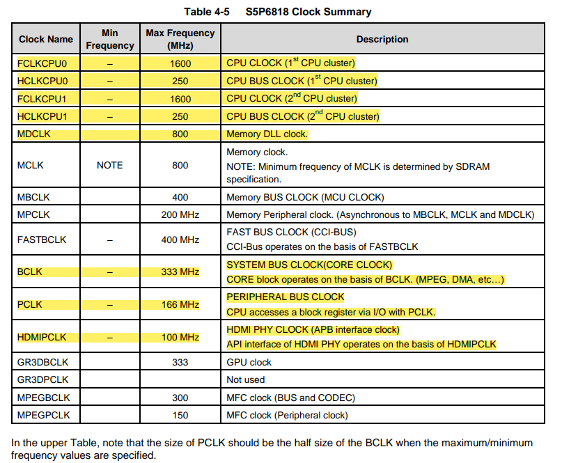
In addition, for generating clocks for internal IPs, the Soc includes 3 clock generator levels with each one serving a specific set of peripherals.
For example, The Clock Generator Level-1 has one clock divider : 8-bit divide registers i.e., up to 256 divide levels. Following peripherals use Level 1 Clock Generator: MIPICSI, PPM, PWMTIMER, SDMMC, SPDIFTX, SSP, UART, VIP.
see section 5 in TRM.
clocks {
compatible = "nexell,s5pxx18,clocks";
reg = <0xc00bb000 0x30000>; This address cannot be understood !! the lowest clk address found in TRM is 0xC006B000 (clk of
USB2HOST) which is lower than 0xc00bb000
#address-cells = <1>;
#size-cells = <1>;
ranges;
PLL and *CLK nodes are unique, as they are providers AND consumers at the same time !!
NEXELL SPECIFIC : the following 7 nodes are supposed to be, not only providers, but also consumers, however no “clocks” property is defined
(which is a mandatory property for every consumer) !! and again, they handle this mis-implementation in the driver clk-s5pxx18-pll.c.
In the beginning of this DTS a node refclk is defined (in a very confusing way), which could’ve been the value for the clock specifier below but … (refclk “is supposed to” correspond to the 24MHz xtal which is the actual input of the PLLs)
pll0: pll0 {
#clock-cells = <0>; Number of cells in a clock specifier; Typically 0 for nodes with a single clock output and 1 for nodes with
multiple clock outputs.
clock-names = "sys-pll0"; This is a consumer property and it must be defined in accordance with the “clocks” property (which
isn’t defined here). The array of strings in this property have a one to one correspondence with the specifiers in the clocks property. The consumer’s driver will use clock-names to match with clock specifiers.
clock-output-names = "pll0"; This is a provider property. it contains an array of names for the output clks that this device
provides. This is the array that is referenced in the consumer’s clock specifier. For example for a consumer that uses this node’s output clk as its input, must define its specifier as follows :
clocks = <&pll0 0>; /* where &pll0 is the phandle of the provider and 0 corresponds to the index of the wanted clk output in the clock-output-names array, here 0 means output “pll0” */
Note that in this case where #clock-cells = <0> i.e., &pll0 provides only one clk, the index 0 specified in the clock specifier can be omitted.
};
pll1: pll1 {
#clock-cells = <0>;
clock-names = "sys-pll1";
clock-output-names = "pll1";
};
pll2: pll2 {
#clock-cells = <0>;
clock-names = "sys-pll2";
clock-output-names = "pll2";
};
pll3: pll3 {
#clock-cells = <0>;
clock-names = "sys-pll3";
clock-output-names = "pll3";
};
NEXELL SPECIFIC : in addition to these 3 nodes, why other system clocks are not defined e.g., sys-mbclk, sys-vpupclk … ?????
After analysis, the following clocks were defined only because they are directly used by some peripherals… The other system clocks are not.
bclk: bclk {
#clock-cells = <0>;
clock-names = "sys-bbclk";
clock-output-names = "bclk";
};
pclk: pclk {
#clock-cells = <0>;
clock-names = "sys-bpclk";
clock-output-names = "pclk";
};
apb_pclk: apb_pclk {
#clock-cells = <0>;
clock-names = "sys-bbclk";
clock-output-names = "apb_pclk";
};
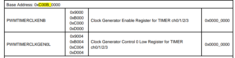
NEXELL SPECIFIC : Again some nexell shit ! here they define properties (cell-id, clk-step, clk-input) that are only for their drivers. This is
not prohibited, but a common way for doing this is to prefix each new property with the vendor’s name i.e., nexell,cell-id = <...>;
cell-id, clk-step and clk-input describes the configuration of the corresponding clock generator level. See section5 in TRM.
timer0:timer@c00b9000 {
#clock-cells = <0>; only one output clk
clock-output-names = "timer0"; called timer0
cell-id = <CLK_ID_TIMER_0>;
reg = <PHYS_BASE_CLK_14 0x1000>;
clk-step = <1>;
clk-input = <CLK_INPUT_TIMER>;
};
timer1:timer@c00bb000 {
#clock-cells = <0>;
clock-output-names = "timer1";
cell-id = <CLK_ID_TIMER_1>;
reg = <PHYS_BASE_CLK_0 0x1000>;
clk-step = <1>;
clk-input = <CLK_INPUT_TIMER>;
};
timer2:timer@c00bc000 {
#clock-cells = <0>;
clock-output-names = "timer2";
cell-id = <CLK_ID_TIMER_2>;
reg = <PHYS_BASE_CLK_1 0x1000>;
clk-step = <1>;
clk-input = <CLK_INPUT_TIMER>;
};
timer3:timer@c00bd000 {
#clock-cells = <0>;
clock-output-names = "timer3";
cell-id = <CLK_ID_TIMER_3>;
reg = <PHYS_BASE_CLK_2 0x1000>;
clk-step = <1>;
clk-input = <CLK_INPUT_TIMER>;
};
uart0:uart@c00a9000 {
#clock-cells = <0>;
clock-output-names = "uart0";
cell-id = <CLK_ID_UART_0>;
reg = <PHYS_BASE_CLK_22 0x1000>;
clk-step = <1>;
clk-input = <CLK_INPUT_UART>;
};
uart1:uart@c00a8000 {
#clock-cells = <0>;
clock-output-names = "uart1";
cell-id = <CLK_ID_UART_1>;
reg = <PHYS_BASE_CLK_24 0x1000>;
clk-step = <1>;
clk-input = <CLK_INPUT_UART>;
};
uart2:uart@c00aa000 {
#clock-cells = <0>;
clock-output-names = "uart2";
cell-id = <CLK_ID_UART_2>;
reg = <PHYS_BASE_CLK_23 0x1000>;
clk-step = <1>;
clk-input = <CLK_INPUT_UART>;
};
uart3:uart@c00ab000 {
#clock-cells = <0>;
clock-output-names = "uart3";
cell-id = <CLK_ID_UART_3>;
reg = <PHYS_BASE_CLK_25 0x1000>;
clk-step = <1>;
clk-input = <CLK_INPUT_UART>;
};
uart4:uart@c006e000 {
#clock-cells = <0>;
clock-output-names = "uart4";
cell-id = <CLK_ID_UART_4>;
reg = <PHYS_BASE_CLK_26 0x1000>;
clk-step = <1>;
clk-input = <CLK_INPUT_UART>;
};
uart5:uart@c0084000 {
#clock-cells = <0>;
clock-output-names = "uart5";
cell-id = <CLK_ID_UART_5>;
reg = <PHYS_BASE_CLK_27 0x1000>;
clk-step = <1>;
clk-input = <CLK_INPUT_UART>;
};
PWM and TIMER clocks !
pwm0:pwm0@c00ba000 {
#clock-cells = <0>;
clock-output-names = "pwm0";
cell-id = <CLK_ID_PWM_0>;
reg = <PHYS_BASE_CLK_13 0x1000>; this is the base address of PWM0, not documented in TRM !!
clk-step = <1>;
clk-input = <CLK_INPUT_PWM>;
};
pwm1:pwm1@c00ba000 {
#clock-cells = <0>;
clock-output-names = "pwm1";
cell-id = <CLK_ID_PWM_1>;
reg = <PHYS_BASE_CLK_13 0x1000>; this is the base address of PWM0 again !! Some sorcery is going on in the driver.
clk-step = <1>;
clk-input = <CLK_INPUT_PWM>;
};
pwm2:pwm2@c00be000 {
#clock-cells = <0>;
clock-output-names = "pwm2";
cell-id = <CLK_ID_PWM_2>;
reg = <PHYS_BASE_CLK_3 0x1000>; this is the base address of PWM1, not documented in TRM
clk-step = <1>;
clk-input = <CLK_INPUT_PWM>;
};
pwm3:pwm3@c00be000 {
#clock-cells = <0>;
clock-output-names = "pwm3";
cell-id = <CLK_ID_PWM_3>;
reg = <PHYS_BASE_CLK_3 0x1000>; this is the base address of PWM1 again !!!! not documented in TRM
clk-step = <1>;
clk-input = <CLK_INPUT_PWM>;
};
pwm4 is not available externally (no pin) nor timer4 btw.
i2c0:i2c@c00ae000 {
#clock-cells = <0>;
clock-output-names = "i2c0";
cell-id = <CLK_ID_I2C_0>;
reg = <PHYS_BASE_CLK_6 0x1000>;
clk-step = <1>;
clk-input = <CLK_INPUT_I2C>;
};
i2c1:i2c@c00af000 {
#clock-cells = <0>;
clock-output-names = "i2c1";
cell-id = <CLK_ID_I2C_1>;
reg = <PHYS_BASE_CLK_7 0x1000>;
clk-step = <1>;
clk-input = <CLK_INPUT_I2C>;
};
i2c2:i2c@c00b0000 {
#clock-cells = <0>;
clock-output-names = "i2c2";
cell-id = <CLK_ID_I2C_2>;
reg = <PHYS_BASE_CLK_8 0x1000>;
clk-step = <1>;
clk-input = <CLK_INPUT_I2C>;
};
i2s0:i2s@c00b2000 {
#clock-cells = <0>;
clock-output-names = "i2s0";
cell-id = <CLK_ID_I2S_0>;
reg = <PHYS_BASE_CLK_15 0x1000>;
clk-step = <2>;
clk-input = <CLK_INPUT_I2S>;
clk-input1 = <CLK_INPUT_I2S_IN1>;
};
i2s1:i2s@c00b3000 {
#clock-cells = <0>;
clock-output-names = "i2s1";
cell-id = <CLK_ID_I2S_1>;
reg = <PHYS_BASE_CLK_16 0x1000>;
clk-step = <2>;
clk-input = <CLK_INPUT_I2S>;
clk-input1 = <CLK_INPUT_I2S_IN1>;
};
i2s2:i2s@c00b4000 {
#clock-cells = <0>;
clock-output-names = "i2s2";
cell-id = <CLK_ID_I2S_2>;
reg = <PHYS_BASE_CLK_17 0x1000>;
clk-step = <2>;
clk-input = <CLK_INPUT_I2S>;
clk-input1 = <CLK_INPUT_I2S_IN1>;
};
sdhc0:sdhc@c00c5000 {
#clock-cells = <0>;
clock-output-names = "sdhc0";
cell-id = <CLK_ID_SDHC_0>;
reg = <PHYS_BASE_CLK_18 0x1000>;
clk-step = <1>;
clk-input = <CLK_INPUT_SDHC>;
};
sdhc1:sdhc@c00cc000 {
#clock-cells = <0>;
clock-output-names = "sdhc1";
cell-id = <CLK_ID_SDHC_1>;
reg = <PHYS_BASE_CLK_19 0x1000>;
clk-step = <1>;
clk-input = <CLK_INPUT_SDHC>;
};
sdhc2:sdhc@c00cd000 {
#clock-cells = <0>;
clock-output-names = "sdhc2";
cell-id = <CLK_ID_SDHC_2>;
reg = <PHYS_BASE_CLK_20 0x1000>;
clk-step = <1>;
clk-input = <CLK_INPUT_SDHC>;
};
spi0:spi@c00ac000 {
#clock-cells = <0>;
clock-output-names = "spi0";
cell-id = <CLK_ID_SPI_0>;
reg = <PHYS_BASE_CLK_37 0x1000>;
clk-step = <1>;
clk-input = <CLK_INPUT_SPI>;
};
spi1:spi@c00ad000 {
#clock-cells = <0>;
cell-id = <CLK_ID_SPI_1>;
reg = <PHYS_BASE_CLK_38 0x1000>;
clk-step = <1>;
clk-input = <CLK_INPUT_SPI>;
clock-output-names = "spi1";
};
spi2:spi@c00a7000 {
#clock-cells = <0>;
cell-id = <CLK_ID_SPI_2>;
reg = <PHYS_BASE_CLK_39 0x1000>;
clk-step = <1>;
clk-input = <CLK_INPUT_SPI>;
clock-output-names = "spi2";
};
vip0:vip@c00c1000 {
#clock-cells = <0>;
cell-id = <CLK_ID_VIP_0>;
reg = <PHYS_BASE_CLK_30 0x1000>;
clk-step = <1>;
clk-input = <CLK_INPUT_VIP0>;
clock-output-names = "vip0";
};
vip1:vip@c00c2000 {
#clock-cells = <0>;
cell-id = <CLK_ID_VIP_1>;
reg = <PHYS_BASE_CLK_31 0x1000>;
clk-step = <1>;
clk-input = <CLK_INPUT_VIP1>;
clock-output-names = "vip1";
};
vip2:vip@c0099000 {
#clock-cells = <0>;
cell-id = <CLK_ID_VIP_2>;
reg = <PHYS_BASE_CLK_40 0x1000>;
clk-step = <1>;
clk-input = <CLK_INPUT_VIP2>;
clock-output-names = "vip2";
};
mipi:mipi@c00ca000 {
#clock-cells = <0>;
cell-id = <CLK_ID_MIPI>;
reg = <PHYS_BASE_CLK_9 0x1000>;
clk-step = <1>;
clk-input = <CLK_INPUT_MIPI>;
clock-output-names = "mipi";
};
gmac:gmac@c00c8000 {
#clock-cells = <0>;
cell-id = <CLK_ID_GMAC>;
reg = <PHYS_BASE_CLK_10 0x1000>;
clk-step = <2>;
clk-input = <CLK_INPUT_GMAC>;
clk-input1 = <CLK_INPUT_GMAC_IN1>;
clock-output-names = "gmac";
src-force = <4>;
};
spdiftx:spdiftx@c00b8000 {
#clock-cells = <0>;
cell-id = <CLK_ID_SPDIF_TX>;
reg = <PHYS_BASE_CLK_11 0x1000>;
clk-step = <1>;
clk-input = <CLK_INPUT_SPDIFTX>;
clock-output-names = "spdif-tx";
};
mpegtsi:mpegtsi@c00b7000 {
#clock-cells = <0>;
cell-id = <CLK_ID_MPEGTSI>;
reg = <PHYS_BASE_CLK_12 0x1000>;
clk-step = <1>;
clk-input = <CLK_INPUT_MPEGTS>;
clock-output-names = "mpeg-tsi";
};
vr:vr@c00c3000 {
#clock-cells = <0>;
cell-id = <CLK_ID_VR>;
reg = <PHYS_BASE_CLK_21 0x1000>;
clk-step = <1>;
clk-input = <CLK_INPUT_VR>;
clock-output-names = "vr";
};
deinterlace:deinterlace@c00b5000 {
#clock-cells = <0>;
cell-id = <CLK_ID_DIT>;
reg = <PHYS_BASE_CLK_28 0x1000>;
clk-step = <1>;
clk-input = <CLK_INPUT_DIT>;
clock-output-names = "deinterlace";
};
ppm:pppm@c00c4000 {
#clock-cells = <0>;
cell-id = <CLK_ID_PPM>;
reg = <PHYS_BASE_CLK_29 0x1000>;
clk-step = <1>;
clk-input = <CLK_INPUT_PPM>;
clock-output-names = "ppm";
};
vpu:vpu@c00c7000 {
#clock-cells = <0>;
cell-id = <CLK_ID_CODA>;
reg = <PHYS_BASE_CLK_33 0x1000>;
clk-step = <1>;
clk-input = <CLK_INPUT_VPU>;
clock-output-names = "vpu";
};
crypto:crypto@c00c6000 {
#clock-cells = <0>;
cell-id = <CLK_ID_CRYPTO>;
reg = <PHYS_BASE_CLK_34 0x1000>;
clk-step = <1>;
clk-input = <CLK_INPUT_CRYPTO>;
clock-output-names = "crypto";
};
scaler:scaler@c00b6000 {
#clock-cells = <0>;
clock-output-names = "scaler";
cell-id = <CLK_ID_CRYPTO>;
reg = <PHYS_BASE_CLK_35 0x1000>;
clk-step = <1>;
clk-input = <CLK_INPUT_SCALER>;
};
pdm:pdm@c00cb000 {
#clock-cells = <0>;
clock-output-names = "pdm";
cell-id = <CLK_ID_PDM>;
reg = <PHYS_BASE_CLK_36 0x1000>;
clk-step = <1>;
clk-input = <CLK_INPUT_PDM>;
};
usbhost:usbhost@c006b000 {
#clock-cells = <0>;
cell-id = <CLK_ID_USB2HOST>;
reg = <PHYS_BASE_CLK_32 0x1000>;
clk-step = <2>;
clk-input = <CLK_INPUT_EHCI>;
clk-input1 = <CLK_INPUT_EHCI_IN1>;
clock-output-names = "usbhost";
clock-frequency = <12000000>; Legacy property for single, fixed frequency clocks
};
otg:otg@6c00b000 {
#clock-cells = <0>;
clock-output-names = "otg";
cell-id = <CLK_ID_USBOTG>;
reg = <PHYS_BASE_CLK_32 0x1000>;
clk-step = <2>;
clk-input = <CLK_INPUT_OTG>;
clk-input1 = <CLK_INPUT_OTG_IN1>;
};
}; END of clock controller
DMA CONTROLLER:
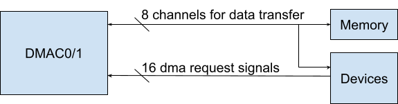
The DMA controller is defined as a child of the amba node, because it is a primecell device and it is directly connected to the amba bus. As the SOC node represents only simple-bus devices, the switch here to amba-bus is required. (It could’ve been possible to define this node outside the soc if wanted)
The ARM Advanced Microcontroller Bus Architecture (AMBA) is an open-standard, on-chip interconnect specification for the connection and management of functional blocks in system-on-a-chip designs.
The S5p6818 specs:
- The S5p6818 implements the AMBA 3 specification, with a PrimeCell® High-Performance Matrix (PL301) AXI3 BUS, an AHB BUS and an APB BUS.
- There are 2 DMAC in S5P6818 and each DMAC has eight channels for data transfer, which can buffer up to 4 words each.
- Each DMAC supports 16 DMA requestors, and generates individually maskable interrupts for Terminal count and transfer error for each channel.
amba {
compatible = "arm,amba-bus";
reg = <0xC0000000 0x2000>; from TRM dmac0 starts at 0xC0000000 and dmac1 starts at 0xC0001000
#address-cells = <1>;
#size-cells = <1>;
interrupt-parent = <&gic>;
ranges;
pl08xdma0:pl08xdma@c0000000 {
compatible = "arm,pl080", "arm,primecell"; This node is an ARM PrimeCell PL080 DMA controller. it can move blocks of memory
contents between memory and peripherals.
arm,primecell-periphid = <0x00041080>; contains the PrimeCell Peripheral ID, it overrides the ID provided by the HW
reg = <PHYS_BASE_DMA0 0x1000>; from 0xC0000000 to 0xC0001000
interrupts = <0 IRQ_DMA0 0>;
#dma-cells = <2>; The number of cells that are required for clients to specify a DMA transfer. In this case, there are two cells: the
dma controller phandel plus the request, or, channel line number e.g.:
i2c1: i2c@1 {
...
dmas = <&dma 2 &dma 3>; /* read and write channels */
dma-names = "rx", "tx";
...
};
dma-channels = <8>; number of dma channels for data transfer
dma-requests = <16>; number of dma request signals
lli-bus-interface-ahb1; Indicates that the DMA controller supports Linked List Item (LLI) transfers through the AHB1 bus interface for the
associated AHB master.
LLI transfers: with an LLI transfer, the DMA controller can read multiple blocks of data from multiple sources and write them to multiple destinations without any additional intervention from the CPU
mem-bus-interface-ahb1; Indicates that the DMA controller supports memory transfers through the AHB1 bus interface for the
associated AHB master.
memcpy-burst-size = <256>; The maximum number of bytes that the DMA controller can transfer in a single burst when
performing a memory copy operation
memcpy-bus-width = <32>; The data bus width that the DMA controller uses when performing memory copy operations
/* slave channels */
ch0 {
slave_bus_id = PL08X_DMA_NAME_UART1_TX; the name of this device channel
slave_periph_buses = <PL08X_AHB2>; The bus or buses that the peripheral is connected to. This information is used by
the DMA controller to determine the memory access mode, bus width, and other parameters that are
required for the data transfer.
};
ch1 {
slave_bus_id = PL08X_DMA_NAME_UART1_RX; the same as ch0
slave_periph_buses = <PL08X_AHB2>;
};
ch2 {
slave_bus_id = PL08X_DMA_NAME_UART0_TX;
slave_periph_buses = <PL08X_AHB2>;
};
ch3 {
slave_bus_id = PL08X_DMA_NAME_UART0_RX;
slave_periph_buses = <PL08X_AHB2>;
};
ch4 {
slave_bus_id = PL08X_DMA_NAME_UART2_TX;
slave_periph_buses = <PL08X_AHB2>;
};
ch5 {
slave_bus_id = PL08X_DMA_NAME_UART2_RX;
slave_periph_buses = <PL08X_AHB2>;
};
ch6 {
slave_bus_id = PL08X_DMA_NAME_SSP0_TX;
slave_periph_buses = <PL08X_AHB2>;
};
ch7 {
slave_bus_id = PL08X_DMA_NAME_SSP0_RX;
slave_periph_buses = <PL08X_AHB2>;
};
ch8 {
slave_bus_id = PL08X_DMA_NAME_SSP1_TX;
slave_periph_buses = <PL08X_AHB2>;
};
ch9 {
slave_bus_id = PL08X_DMA_NAME_SSP1_RX;
slave_periph_buses = <PL08X_AHB2>;
};
ch10 {
slave_bus_id = PL08X_DMA_NAME_SSP2_TX;
slave_periph_buses = <PL08X_AHB2>;
};
ch11 {
slave_bus_id = PL08X_DMA_NAME_SSP2_RX;
slave_periph_buses = <PL08X_AHB2>;
};
ch12 {
slave_bus_id = PL08X_DMA_NAME_I2S0_TX;
slave_periph_buses = <PL08X_AHB2>;
};
ch13 {
slave_bus_id = PL08X_DMA_NAME_I2S0_RX;
slave_periph_buses = <PL08X_AHB2>;
};
ch14 {
slave_bus_id = PL08X_DMA_NAME_I2S1_TX;
slave_periph_buses = <PL08X_AHB2>;
};
ch15 {
slave_bus_id = PL08X_DMA_NAME_I2S1_RX;
slave_periph_buses = <PL08X_AHB2>;
};
};
pl08xdma1:pl08xdma@c0001000 { the same as dma0
compatible = "arm,pl080", "arm,primecell";
arm,primecell-periphid = <0x00041080>;
reg = <PHYS_BASE_DMA1 0x1000>;
interrupts = <0 IRQ_DMA1 0>;
#dma-cells = <2>;
dma-channels = <8>;
dma-requests = <16>;
lli-bus-interface-ahb1;
mem-bus-interface-ahb1;
memcpy-burst-size = <256>;
memcpy-bus-width = <32>;
/* slave channels */
ch0 {
slave_bus_id = PL08X_DMA_NAME_I2S2_TX;
slave_periph_buses = <PL08X_AHB2>;
};
ch1 {
slave_bus_id = PL08X_DMA_NAME_I2S2_RX;
slave_periph_buses = <PL08X_AHB2>;
};
ch2 {
slave_bus_id = PL08X_DMA_NAME_AC97_PCMOUT;
slave_periph_buses = <PL08X_AHB2>;
};
ch3 {
slave_bus_id = PL08X_DMA_NAME_AC97_PCMIN;
slave_periph_buses = <PL08X_AHB2>;
};
ch4 {
slave_bus_id = PL08X_DMA_NAME_AC97_MICIN;
slave_periph_buses = <PL08X_AHB2>;
};
ch5 {
slave_bus_id = PL08X_DMA_NAME_SPDIFRX;
slave_periph_buses = <PL08X_AHB2>;
};
ch6 {
slave_bus_id = PL08X_DMA_NAME_SPDIFTX;
slave_periph_buses = <PL08X_AHB2>;
};
ch7 {
slave_bus_id = PL08X_DMA_NAME_MPEGTSI0;
slave_periph_buses = <PL08X_AHB2>;
};
ch8 {
slave_bus_id = PL08X_DMA_NAME_MPEGTSI1;
slave_periph_buses = <PL08X_AHB2>;
};
ch9 {
slave_bus_id = PL08X_DMA_NAME_MPEGTSI2;
slave_periph_buses = <PL08X_AHB2>;
};
ch10 {
slave_bus_id = PL08X_DMA_NAME_MPEGTSI3;
slave_periph_buses = <PL08X_AHB2>;
};
ch11 {
slave_bus_id = PL08X_DMA_NAME_CRYPTO_BR;
slave_periph_buses = <PL08X_AHB2>;
};
ch12 {
slave_bus_id = PL08X_DMA_NAME_CRYPTO_BW;
slave_periph_buses = <PL08X_AHB2>;
};
ch13 {
slave_bus_id = PL08X_DMA_NAME_CRYPTO_HR;
slave_periph_buses = <PL08X_AHB2>;
};
ch14 { this channel along with ch15 are marked as reserved in the TRM !!
slave_bus_id = PL08X_DMA_NAME_PDM;
slave_periph_buses = <PL08X_AHB2>;
};
};
};
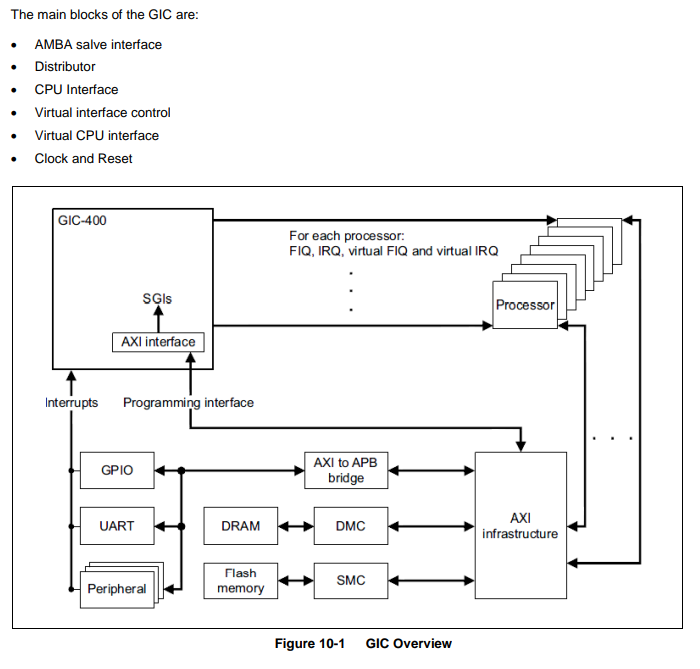
ARM GIC Generic Interrupt Controller:
https://www.kernel.org/doc/Documentation/devicetree/bindings/interrupt-controller/arm%2Cgic.txt
-The S5P6818’s GIC supports 4 interrupts types:
- 16 Software Generated Interrupt (SGIs)
- 6 external Private Peripheral Interrupt (PPIs) for each processor.
- 1 internal PPI for each processor
- 128 Shared Peripheral Interrupt (SPIs)
-The GIC includes interrupt grouping functionality that supports:
- Configuring each interrupt as either Group 0 or Group 1
- Signaling Group 0 interrupts to the target processor using either the IRQ or the FIQ exception request
- Signaling Group 1 interrupts to the target processor using the IRQ exception request only
-Interrupt types:
- Peripheral Interrupt: This is an interrupt asserted by a signal to the GIC. The GIC architecture defines the following types of peripheral interrupt:
- Private Peripheral Interrupt (PPI): This is a peripheral interrupt that is specific to a single processor.
- Shared Peripheral Interrupt (SPI): This is a peripheral interrupt that the Distributor can route to any of a specified combination of processors.
- Software-Generated Interrupt (SGI): This is an interrupt generated by software writing to a GICD_SGIR register in the GIC. The system uses SGIs for inter processor communication.
- Virtual Interrupt: In a GIC that implements the GIC Virtualization Extensions, an interrupt that targets a virtual machine running on a processor, and is typically signaled to the processor by the connected virtual CPU interface.
-Handling interrupts:
In a multiprocessor implementation, there are two models for handling interrupts:
- 1-N model: Only one processor handles this interrupt. The system must implement a mechanism to determine which processor handles an interrupt that is programmed to target more than one processor.
- N-N model: All processors receive the interrupt independently. When a processor acknowledges the interrupt, the interrupt pending state is cleared only for that processor. The interrupt remains pending for the other processors.
The following are the IRQ ids of the SPI interrupts linked to the s5p6818’s gic:
0 => MCUSTOP interrupt
1 => DMA0 interrupt
2 => DMA1 interrupt
3 => CLKPWRPWR interrupt
4 => CLKPWRALIVE interrupt
5 => CLKPWRRTC interrupt
6 => UART1 interrupt
7 => UART0 interrupt
8 => UART2 interrupt
9 => UART3 interrupt
10 => UART4 interrupt
11 => UART5 interrupt
12 => SSP0 interrupt
13 => SSP1 interrupt
14 => SSP2 interrupt
15 => I2C0 interrupt
16 => I2C1 interrupt
17 => I2C2 interrupt
18 => DEINTERLACE interrupt
19 => SCALER interrupt
20 => AC97 interrupt
21 => SPDIFRX interrupt
22 => SPDIFTX interrupt
23 => TIMER0 interrupt
24 => TIMER1 interrupt
25 => TIMER2 interrupt
26 => TIMER3 interrupt
27 => PWM0 interrupt
28 => PWM1 interrupt
29 => PWM2 interrupt
30 => PWM3 interrupt
31 => WDT interrupt
32 => MPEGTSI interrupt
33 => DISPLAYDUALDISPLAYPRIM interrupt
34 => DISPLAYDUALDISPLAYSECOND interrupt
35 => DISPLAYRESCONV interrupt
36 => DISPLAYHDMI interrupt
37 => VIP0 interrupt
38 => VIP1 interrupt
39 => MIPI interrupt
40 => 3D GPU interrupt
41 => ADC interrupt
42 => PPM interrupt
43 => SDMMC0 interrupt
44 => SDMMC1 interrupt
45 => SDMMC2 interrupt
46 => CODA960HOST interrupt
47 => CODA960JPG interrupt
48 => GMAC interrupt
49 => USB20OTG interrupt
50 => USB20HOST interrupt
51 => N/A
52 => N/A
53 => GPIOA interrupt
54 => GPIOB interrupt
55 => GPIOC interrupt
56 => GPIOD interrupt
57 => GPIOE interrupt
58 => CRYPTO interrupt
59 => N/A
60 => TMU0 interrupt
61 => TMU1 interrupt
62-71 => N/A
72 => VIP2 Interrupt
gic:interrupt-controller@c0009000 {
compatible = "arm,gic-400"; it's a GIC version 4
interrupt-controller; your excellence, welcome !
#interrupt-cells = <3>; Specifies the number of cells needed to encode an interrupt source in client devices.
The 1st cell is the interrupt type; 0 for SPI interrupts, 1 for PPI interrupts.
The 2nd cell contains the interrupt number for the interrupt type. SPI interrupts are in the range [0-987]. PPI interrupts are in the range [0-15].
The 3rd cell is the flags, encoded as follows:
bits[3:0] trigger type and level flags.
1 = low-to-high edge triggered
2 = high-to-low edge triggered (invalid for SPIs)
4 = active high level-sensitive
8 = active low level-sensitive (invalid for SPIs).
bits[15:8] PPI interrupt cpu mask. Each bit corresponds to each of the 8 possible cpus attached to the GIC. A bit set to '1' indicates the interrupt is wired to that CPU. Only valid for PPI interrupts. Also note that the configurability of PPI interrupts is IMPLEMENTATION DEFINED and as such not guaranteed to be present (most SoC available in 2014 seem to ignore the setting of this flag and use the hardware default value).
reg = <0xC0009000 0x1000>, <0xC000a000 0x100>; Specifies base physical address(s) and size of the GIC registers. The first region is
the GIC distributor register base and size. The 2nd region is the GIC cpu interface register base and size.
};
TIMERs:
The S5P6818 has five 32-bit Pulse Width Modulation (PWM) timers.
These Timers generate internal interrupts for the ARM subsystem.
Timers 0, 1, 2 and 3 include a PWM function that drives an external I/O signal.
The PWM in Timer 0 has an optional dead-zone generator capability to support a large current device.
Timer 4 is an internal timer without output pins.
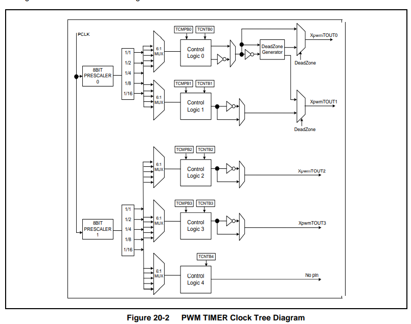
NEXELL SPECIFIC : In the following node it may seem that ONLY timer1 is defined (IRQ_TIMER1), however, in fact both timer0 and 1 are described in the below node (genius developers), but, why not, as long as they are the one making the driver (drivers/clocksource/s5pxx18_timer.c)… Timers 2,3 and 4 are not defined at all !
Here, clksource and clkevent properties are used to describe the role of each timer i.e., timer0 is handled as a clocksource under the kernel, while timer1 is handled as a clockchip/event…
Well, what the heck is a clocksource/clockevent ???
Under the Linux kernel, timers can be set up to have roles (via frameworks):
- a clocksource: The main goal of the clocksource is to provide a timeline. For example, issuing the command 'date' on a Linux system will eventually read the clock source to determine exactly what time it is ! Each clock source provides a monotonic atomic counter (but doesn’t generate any event/interrupt), the Linux kernel uses them to provide accurate timing information to various subsystems.
- a clockevent: Clock events are the conceptual reverse of clock sources. The main goal of this, is to manage clock event devices or in other words - to manage devices that allow to register an event i.e., an interrupt, that is going to happen at a defined point of time in the future.(This is why (IRQ_TIMER1 is defined but not IRQ_TIMER0 !)
for more info https://0xax.gitbooks.io/linux-insides/content/Timers/linux-timers-5.html
timer@c0017000 {
compatible = "nexell,s5p6818-timer";
reg = <PHYS_BASE_TIMER 0x1000>; 0xC0017000 base address and 0x1000 size
interrupts = <0 IRQ_TIMER1 0>; SPI interrupt from timer1, with Id 24 and no flags !
clksource = <0>; NEXELL SPECIFIC
clkevent = <1>; NEXELL SPECIFIC
clocks = <&timer0>, <&timer1>, <&pclk>; pclk is the input clock before prescaller, timer0 and timer1 are the clockenb for the two
controllers.
clock-names = "timer0", "timer1", "pclk";
};
TieOFF:
In an embedded System-on-Chip (SoC), tie-off registers are used to ensure that a signal has a defined logic value when it is not being actively driven by a driver circuit.
Tie-off registers are usually implemented as flip-flops with a fixed value that is programmed during the manufacturing process of the chip. The purpose of these flip-flops is to provide a known value to an input pin of a module that is not being actively driven by any other logic circuit. Without tie-off registers, such unconnected inputs could float to an unknown value, causing unpredictable behavior of the chip.
These registers are an essential part of the design of an SoC, ensuring the correct and reliable behavior of the chip under different operating conditions.
In the S5P6818, the Tieoff block includes special function registers for ARM, HDMI, DRAM controller, UART, USB2.0 HOST controller/ Phy, USB2.0 OTG controller/ Phy, Ethernet controller, AXI buses and the internal SRAM timing margin controls.
tieoff@c0011000 {
compatible = "nexell,tieoff";
reg = <PHYS_BASE_TIEOFF 0x1000>;
};
Dynamic Voltage Frequency Scaling (DVFS):
The CPU DVFS subsystem is responsible for adjusting the frequency and voltage of the CPU when the CPU is running, so that the power consumption of the CPU is as low as possible under the premise of satisfying performance.
It mainly solves two problems: when to adjust frequency and voltage, and how to adjust frequency and voltage.
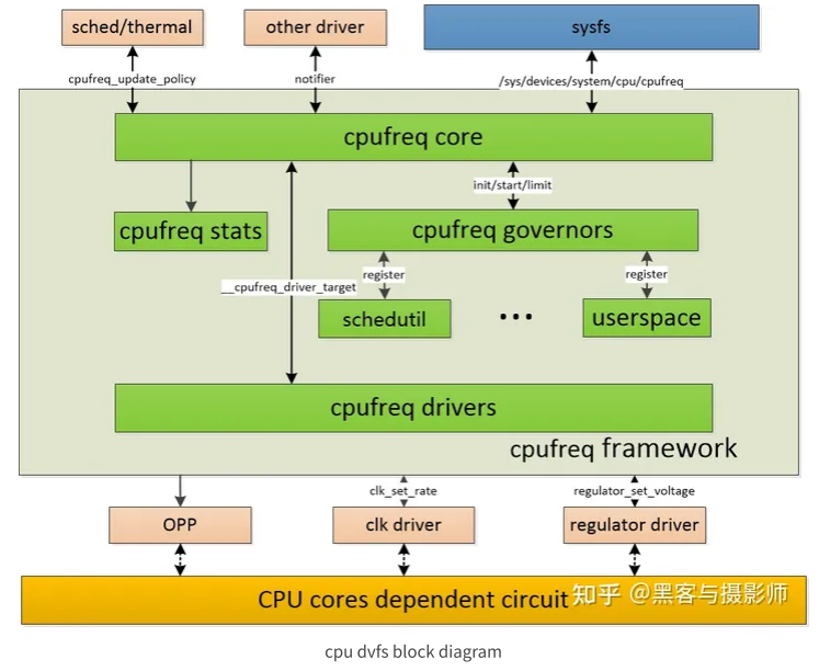
- cpufreq core: is the core module of the cpufreq framework, similar to other frameworks of the kernel, and mainly implements three types of functions
- The public logic and interface of abstract frequency modulation and voltage regulation mainly revolve around the three data structures of struct cpufreq_driver, struct cpufreq_policy and struct cpufreq_governor.
- Provide a unified interface to user space in the form of sysfs, and provide frequency change notifications to other drivers in the form of notifier.
- Provide a driver framework for CPU frequency and voltage control to facilitate the development of the underlying driver; at the same time, provide a governor framework for implementing different frequency adjustment mechanisms.
- cpufreq governor: Responsible for various strategies for frequency modulation and voltage regulation. Each governor calculates the frequency in a different way. According to the frequency range and parameters (threshold, etc.) provided, the appropriate frequency is calculated.
- userspace: The user can adjust the operating frequency and voltage by operating the scaling_setspeed file node.
- ondemand: Dynamically adjust the CPU frequency and voltage according to the current CPU usage. Sched triggers load estimation by calling the callback function registered by ondemand. It samples the system load at a certain time interval and adjusts the frequency and voltage of the cpu as needed. If the current cpu utilization exceeds the set threshold, it will immediately be tuned to the maximum frequency. FM is fast, but not precise enough.
- conservative: Similar to ondemand, it will be smoothed during FM adjustment to prevent jumping back and forth between the maximum and minimum frequencies. When adjusting, it will be adjusted in a certain step, instead of directly adjusting to the target value. At the same time, the system load will be calculated periodically to determine what frequency to adjust.
- schedutil: By registering its own frequency regulation strategy to the hook, when the load changes, the hook will be called, and then the frequency regulation decision can be made or the frequency regulation action can be executed. The previous frequency modulation strategies all use periodic sampling to calculate the CPU load, which has a lag and limited accuracy, but schedutil can use PELT (per entity load tracking) or WALT (window assist load tracking) to accurately calculate the task load. If the fast_switch function is supported, frequency modulation can be performed directly in the interrupt context.
- cpufreq driver: responsible for the implementation of platform-related frequency and voltage regulation mechanisms, based on cpu subsystem driver, OPP, clock driver, regulator driver and other modules, providing control over CPU frequency and voltage.
- cpufreq stats: Responsible for statistics of frequency modulation information and running time of each frequency point, and provide statistics related to cpufreq of each cpu.
This node is not complete, it is missing the supply regulator, and it should be completed in the board device tree.
dynamic-freq@bb000 {
compatible = "nexell,s5pxx18-cpufreq";
reg = <0xc00bb000 0x30000>; From TRM, 0xc00bb000 points to the Clock Generator Enable Register for TIMER ch1 !!!!!!!!!
The reg property is not needed for this cpufreq driver… can’t know why it is defined.
};
UART Controller
The S5P6818 has 6 UART ports.
serial0:serial@c00a1000 {
compatible = "nexell,s5p6818-uart";
reg = <PHYS_BASE_UART0 0x1000>; base address
interrupts = <0 IRQ_UART0 0>; SPI interrupt
clock-names = "uart", "clk_uart_baud0"; bus clock + baudrate clock (the same)
clocks = <&uart0>, <&uart0>;
resets = <&nexell_reset RESET_ID_UART0>; phandle to the reset controller provider, plus the rest signal id/offset
reset-names = "uart-reset";
soc,tieoff = <NX_TIEOFF_UART0_USESMC 0>, tieoff registers to enable the controller
<NX_TIEOFF_UART0_SMCTXENB 0>,
<NX_TIEOFF_UART0_SMCRXENB 0> ;
pinctrl-names = "default";
pinctrl-0 = <&serial0_pin>; pin configuration
status = "disabled";
};
serial1:serial@c00a0000 {
compatible = "nexell,s5p6818-uart";
reg = <PHYS_BASE_UART1 0x1000>;
interrupts = <0 IRQ_UART1 0>;
clock-names = "uart", "clk_uart_baud0";
clocks = <&uart1>, <&uart1>;
resets = <&nexell_reset RESET_ID_UART1>;
reset-names = "uart-reset";
soc,tieoff = <NX_TIEOFF_UART1_USESMC 0>,
<NX_TIEOFF_UART1_SMCTXENB 0>,
<NX_TIEOFF_UART1_SMCRXENB 0> ;
pinctrl-names = "default";
pinctrl-0 = <&serial1_pin>;
status = "disabled";
};
serial2:serial@c00a2000 {
compatible = "nexell,s5p6818-uart";
reg = <PHYS_BASE_UART2 0x1000>;
interrupts = <0 IRQ_UART2 0>;
clock-names = "uart", "clk_uart_baud0";
clocks = <&uart2>, <&uart2>;
resets = <&nexell_reset RESET_ID_UART2>;
reset-names = "uart-reset";
soc,tieoff = <NX_TIEOFF_UART2_USESMC 0>,
<NX_TIEOFF_UART2_SMCTXENB 0>,
<NX_TIEOFF_UART2_SMCRXENB 0> ;
pinctrl-names = "default";
pinctrl-0 = <&serial2_pin>;
status = "disabled";
};
serial3:serial@c00a3000 {
compatible = "nexell,s5p6818-uart";
reg = <PHYS_BASE_UART3 0x1000>;
interrupts = <0 IRQ_UART3 0>;
clock-names = "uart", "clk_uart_baud0";
clocks = <&uart3>, <&uart3>;
resets = <&nexell_reset RESET_ID_UART3>;
reset-names = "uart-reset";
soc,tieoff = <NX_TIEOFF_UART3_USESMC 0>,
<NX_TIEOFF_UART3_SMCTXENB 0>,
<NX_TIEOFF_UART3_SMCRXENB 0> ;
pinctrl-names = "default";
pinctrl-0 = <&serial3_pin>;
status = "disabled";
};
serial4:serial@c006d000 {
compatible = "nexell,s5p6818-uart";
reg = <PHYS_BASE_UART4 0x1000>;
interrupts = <0 IRQ_UART4 0>;
clock-names = "uart", "clk_uart_baud0";
clocks = <&uart4>, <&uart4>;
resets = <&nexell_reset RESET_ID_UART4>;
reset-names = "uart-reset";
soc,tieoff = <NX_TIEOFF_UART4_USESMC 0>,
<NX_TIEOFF_UART4_SMCTXENB 0>,
<NX_TIEOFF_UART4_SMCRXENB 0> ;
pinctrl-names = "default";
pinctrl-0 = <&serial4_pin>;
status = "disabled";
};
serial5:serial@c006f000 {
compatible = "nexell,s5p6818-uart";
reg = <PHYS_BASE_UART5 0x1000>;
interrupts = <0 IRQ_UART5 0>;
clock-names = "uart", "clk_uart_baud0";
clocks = <&uart5>, <&uart5>;
resets = <&nexell_reset RESET_ID_UART5>;
reset-names = "uart-reset";
soc,tieoff = <NX_TIEOFF_UART5_USESMC 0>,
<NX_TIEOFF_UART5_SMCTXENB 0>,
<NX_TIEOFF_UART5_SMCRXENB 0> ;
pinctrl-names = "default";
pinctrl-0 = <&serial5_pin>;
status = "disabled";
};
RESET Controller:
used to reset different IPs inside the chip. Each peripheral has a unique reg.
= Reset consumers =
Required properties:
- resets: List of phandle and reset specifier pairs, one pair for each reset signal that affects the device, or that the device manages. Note: if the reset provider specifies '0' for #reset-cells, then only the phandle portion of the pair will appear.
nexell_reset:reset@c0012000 {
#reset-cells = <1>; provider property. Number of cells in a reset specifier; Typically 0 for nodes with a single reset output and 1 for nodes with
multiple reset outputs.
compatible = "nexell,s5pxx18-reset";
reg = <0xC0012000 0x3>; all reset signals are routed to 3 regs. Each bit corresponds to a reset line.
status = "okay";
};
PWM Controller:
pwm:pwm@c0018000 {
compatible = "nexell,s5p6818-pwm";
reg = <PHYS_BASE_PWM 0x1000>;
reset-names = "pwm-reset";
resets = <&nexell_reset RESET_ID_PWM>; phandle to the reset controller provider, plus the rest signal id/offset
clock-names = "timers", "pwm-tclk0", "pwm-tclk1";
clocks = <&pclk>, <&pwm0>, <&pwm2>; to understand the clock tree, refer to the timer node seen previously
#pwm-cells = <3>; number of cells used for the specifier in pwm consumers. Generally, 1st is the pwm pin/channel, the second cell is the
pwm periode in nanoseconds and the third cell is a flag for pwm polarity i.e., PWM_POLARITY_INVERTED
pinctrl-names = "default";
pinctrl-0 = <&pwm0_pin &pwm1_pin &pwm2_pin &pwm3_pin>;
samsung,pwm-outputs = <0>, <1>, <2>, <3>; list of PWM channels that have an output pin
status = "disabled";
};
I2C Controller:
The S5P6818 application processor supports 3 multi-master I2C bus serial interfaces.
i2c_0:i2c@c00a4000 {
compatible = "nexell,s5p6818-i2c";
reg = <PHYS_BASE_I2C0 0x100>;
interrupts = <0 IRQ_I2C0 0>;
clock-names = "i2c";
clocks = <&i2c0>;
samsung,i2c-sda-delay = <100>;
samsung,i2c-max-bus-freq = <100000>; 100Kbit/s is max freq in standard mode
samsung,i2c-slave-addr = <0x66>;
resets = <&nexell_reset RESET_ID_I2C0>;
reset-names = "i2c-reset";
pinctrl-names = "default";
pinctrl-0 = <&i2c0_pin>;
status = "disabled";
};
i2c_1:i2c@c00a5000 {
compatible = "nexell,s5p6818-i2c";
reg = <PHYS_BASE_I2C1 0x100>;
interrupts = <0 IRQ_I2C1 0>;
clock-names = "i2c";
clocks = <&i2c1>;
samsung,i2c-sda-delay = <100>;
samsung,i2c-max-bus-freq = <100000>;
samsung,i2c-slave-addr = <0x66>;
resets = <&nexell_reset RESET_ID_I2C1>;
reset-names = "i2c-reset";
pinctrl-names = "default";
pinctrl-0 = <&i2c1_pin>;
status = "disabled";
};
i2c_2:i2c@c00a6000 {
compatible = "nexell,s5p6818-i2c";
reg = <PHYS_BASE_I2C2 0x100>;
interrupts = <0 IRQ_I2C2 0>;
clock-names = "i2c";
clocks = <&i2c2>;
samsung,i2c-sda-delay = <100>;
samsung,i2c-max-bus-freq = <100000>;
samsung,i2c-slave-addr = <0x66>;
resets = <&nexell_reset RESET_ID_I2C2>;
reset-names = "i2c-reset";
pinctrl-names = "default";
pinctrl-0 = <&i2c2_pin>;
status = "disabled";
};
MMC Controller:
Synopsys Designware Mobile Storage Host Controller (DW-MSHC)
https://www.kernel.org/doc/Documentation/devicetree/bindings/mmc/synopsys-dw-mshc.txt
The MSHC is used to interface a SoC with storage medium such as eMMC or SD/MMC cards.
The S5P6818 supports 3 channels of SD/MMC.
dw_mmc_2:dw_mmc@c0069000 {
compatible = "nexell,s5p6818-dw-mshc";
interrupts = <0 IRQ_SDMMC2 0>;
#address-cells = <1>;
#size-cells = <0>;
reg = <PHYS_BASE_SDMMC2 0x1000>;
resets = <&nexell_reset RESET_ID_SDMMC2>;
reset-names = "dw_mmc-reset";
clock-names = "biu","ciu";
clocks = <&sdhc2>, <&sdhc2>;
pinctrl-names = "default";
pinctrl-0 = <&sdmmc2_cclk &sdmmc2_cmd &sdmmc2_bus4>;
fifo-detph = <0x20>;
status = "disabled";
};
dw_mmc_1:dw_mmc@c0068000 {
compatible = "nexell,s5p6818-dw-mshc";
interrupts = <0 IRQ_SDMMC1 0>;
#address-cells = <1>;
#size-cells = <0>;
reg = <PHYS_BASE_SDMMC1 0x1000>;
resets = <&nexell_reset RESET_ID_SDMMC1>;
reset-names = "dw_mmc-reset";
clock-names = "biu","ciu";
clocks = <&sdhc1>, <&sdhc1>;
pinctrl-names = "default";
pinctrl-0 = <&sdmmc1_cclk &sdmmc1_cmd &sdmmc1_bus4>;
fifo-detph = <0x20>;
status = "disabled";
};
dw_mmc_0:dw_mmc@c0062000 {
compatible = "nexell,s5p6818-dw-mshc";
interrupts = <0 IRQ_SDMMC0 0>;
#address-cells = <1>;
#size-cells = <0>;
reg = <PHYS_BASE_SDMMC0 0x1000>;
resets = <&nexell_reset RESET_ID_SDMMC0>;
reset-names = "dw_mmc-reset";
clock-names = "biu", "ciu";
clocks = <&sdhc0>, <&sdhc0>;
pinctrl-names = "default";
pinctrl-0 = <&sdmmc0_cclk &sdmmc0_cmd &sdmmc0_bus4>;
fifo-detph = <0x20>;
status = "disabled";
};
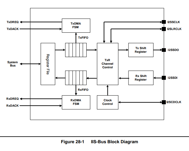
I2S Controller:
The S5P6818 has 3 I2S ports.
i2s_0:i2s@c0055000 {
compatible = "nexell,nexell-i2s";
reg = <PHYS_BASE_I2S0 0x1000>;
dmas = <&pl08xdma0 12 0>, <&pl08xdma0 13 0>; use pl08xdma0 controller with two request IDs : 12 and 13 for Tx and Rx respectively
(the 0 field is ignored by the controller !! as #dma-cells=2)
dma-names = "tx", "rx";
clocks = <&i2s0>;
clock-names = "i2s0";
resets = <&nexell_reset RESET_ID_I2S0>;
reset-names = "i2s-reset";
pinctrl-names = "default";
pinctrl-0 = <&i2s0_bus>;
master-mode = <1>; 0(slave mode), 1(i2s master mode).
mclk-in = <0>; mclk-in source : 0(internal), 1(external)
trans-mode = <0>; 0(i2s mode), 1(MSB-justified) or 2(LSB-justified)
frame-bit = <32>; Select frame bit. (16/24/32/48 fs)
sample-rate = <48000>; Select sample rate. (8000~192000hz)
pre-supply-mclk = <1>; Select pre supply mclk support. 0(control when i2s start/stop), 1(always on)
status = "disabled";
};
i2s_1:i2s@c0056000 {
compatible = "nexell,nexell-i2s";
reg = <PHYS_BASE_I2S1 0x1000>;
dmas = <&pl08xdma0 14 0>, <&pl08xdma0 15 0>;
dma-names = "tx", "rx";
clocks = <&i2s1>;
clock-names = "i2s1";
resets = <&nexell_reset RESET_ID_I2S1>;
reset-names = "i2s-reset";
pinctrl-names = "default";
pinctrl-0 = <&i2s1_bus>;
master-mode = <1>;
mclk-in = <0>;
trans-mode = <0>;
frame-bit = <32>;
sample-rate = <48000>;
pre-supply-mclk = <1>;
status = "disabled";
};
i2s_2:i2s@c0057000 {
compatible = "nexell,nexell-i2s";
reg = <PHYS_BASE_I2S2 0x1000>;
dmas = <&pl08xdma1 0 0>, <&pl08xdma1 1 0>;
dma-names = "tx", "rx";
clocks = <&i2s2>;
clock-names = "i2s2";
resets = <&nexell_reset RESET_ID_I2S2>;
reset-names = "i2s-reset";
pinctrl-names = "default";
pinctrl-0 = <&i2s2_bus>;
master-mode = <1>;
mclk-in = <0>;
trans-mode = <0>;
frame-bit = <32>;
sample-rate = <48000>;
pre-supply-mclk = <1>;
status = "disabled";
};
USB Phy Controller:
The S5p6818 USB phy can be configured to have one OTG port and one of the following host ports:
- 1 Enhanced Host Controller Interface (EHCI) i.e. USB2.2 + 1 High-Speed Inter-Chip (HSIC), Version 1.0
- 1 Open Host Controller Interface (OHCI) i.e. USB1.1 + 1 High-Speed Inter-Chip (HSIC), Version 1.0
nexell_usbphy: nexell-usbphy@c0012000 {
compatible = "nexell,nexell-usb2-phy";
reg = <PHYS_BASE_TIEOFF 0x100>; tieoff regs for enabling/configuring the phy
clocks = <&usbhost>;
clock-names = "phy";
#phy-cells = <1>;
status = "disabled";
};
ehci@c0030000 {
compatible = "nexell,nexell-ehci";
reg = <PHYS_BASE_EHCI 0x10000>;
interrupts = <0 IRQ_USB20HOST 0>;
clocks = <&usbhost>;
clock-names = "usbhost";
resets = <&nexell_reset RESET_ID_USB20HOST>;
reset-names = "usbhost-reset";
status = "disabled";
#address-cells = <1>;
#size-cells = <0>;
port@0 {
reg = <0>;
phys = <&nexell_usbphy 1>; 1 -> USB host ("host")
status = "disabled";
};
port@1 {
reg = <1>;
phys = <&nexell_usbphy 2>; 2 -> HSIC0 ("hsic0")
status = "disabled";
};
};
ohci@c0020000 {
compatible = "nexell,nexell-ohci";
reg = <PHYS_BASE_OHCI 0x10000>;
interrupts = <0 IRQ_USB20HOST 0>;
clocks = <&usbhost>;
clock-names = "usbhost";
resets = <&nexell_reset RESET_ID_USB20HOST>;
reset-names = "usbhost-reset";
status = "disabled";
#address-cells = <1>;
#size-cells = <0>;
port@0 {
reg = <0>;
phys = <&nexell_usbphy 1>; 1 -> USB host ("host")
status = "disabled";
};
};
dwc2otg@c0040000 {
compatible = "nexell,nexell-dwc2otg"; DesignWare HS OTG USB 2.0 controller
reg = <PHYS_BASE_HSOTG 0x11000>;
interrupts = <0 IRQ_USB20OTG 0>;
clocks = <&otg>;
clock-names = "otg";
resets = <&nexell_reset RESET_ID_USB20OTG>;
reset-names = "usbotg-reset";
phys = <&nexell_usbphy 0>; 0 - USB device ("device")
phy-names = "usb2-phy";
dr_mode = "otg"; shall be one of "host", "peripheral" and "otg"
g-use-dma = <1>;
g-rx-fifo-size = <1064>; size of rx fifo size in gadget mode.
g-np-tx-fifo-size = <512>; size of non-periodic tx fifo size in gadget mode.
g-tx-fifo-size = <512 512 256 256 256 256 256 256 256
256 256 256 256 256 256>; size of periodic tx fifo per endpoint (except ep0) in gadget mode
status = "disabled";
};
Gigabit Ethernet Media Access Controller (GMAC):
The S5p6818 gmac supports 10/100/1000 Mbps data transfer rates, and it has Reduced Gigabit Media Independent Interface (RGMII) with External PHY chip.
gmac0:ethernet@c0060000 {
compatible = "nexell,s5p6818-gmac";
clocks = <&pclk>, <&gmac>;
clock-names = "stmmaceth", "nexell_gmac_tx";
resets = <&nexell_reset RESET_ID_DWC_GMAC>;
reset-names = "stmmaceth";
reg = <PHYS_BASE_GMAC 0x2000>;
interrupt-parent = <&gic>;
interrupts = <0 IRQ_GMAC 0>;
interrupt-names = "macirq";
mac-address = [000000000000]; Filled in by U-Boot
phy-mode = "rgmii";
snps,multicast-filter-bins = <256>;
status = "disable";
};
Analog Digital Converter (ADC):
0 to 1.8 V 12-bit analog-to-digital converter (ADC) with 8-ch analog input MUX and level-shifters for low-voltage digital interface. It converts single-ended analog input signals to 12-bit digital output codes at a maximum conversion rate of 1MSPS.
adc:adc@c0053000 {
compatible = "nexell,s5p6818-adc";
reg = <PHYS_BASE_ADC 0x1000>;
interrupts = <0 IRQ_ADC 0>;
resets = <&nexell_reset RESET_ID_ADC>;
reset-names = "adc-reset";
clocks = <&pclk>;
clock-names = "adc";
sample_rate = <200000>;
#io-channel-cells = <1>; Number of cells in an IIO specifier; 0 for nodes with a single IIO output and 1 for nodes with multiple
IIO outputs.
status = "disabled";
};
Serial Peripheral Interface (SPI) and Synchronous Serial Protocol (SSP) Controller:
The S5P6818 has 3 SPI/SSP ports and it can operate in Master and Slave mode.
spi_0:spi@c005b000 {
compatible = "c";
reg = <PHYS_BASE_SSP0 0x100>;
interrupts = <0 IRQ_SSP0 0>;
dmas = <&pl08xdma0 6 0>, <&pl08xdma0 7 0>;
dma-names = "tx", "rx";
resets = <&nexell_reset RESET_ID_SSP0_P>,
<&nexell_reset RESET_ID_SSP0>;
reset-names = "pre-reset","spi-reset";
#address-cells = <1>;
#size-cells = <0>;
samsung,spi-src-clk = <0>;
num-cs = <1>;Specifies the number of chip select lines supported
clocks = <&spi0>, <&spi0>;
clock-names = "spi", "spi_busclk0";
pinctrl-names = "default";
pinctrl-0 = <&spi0_bus>;
status ="disable";
};
spi_1:spi@c005c000 {
compatible = "nexell,s5p6818-spi";
reg = <PHYS_BASE_SSP1 0x100>;
interrupts = <0 IRQ_SSP1 0>;
dmas = <&pl08xdma0 8 0>, <&pl08xdma0 9 0>;
dma-names = "tx", "rx";
resets = <&nexell_reset RESET_ID_SSP1_P>,
<&nexell_reset RESET_ID_SSP1>;
reset-names = "pre-reset","spi-reset";
#address-cells = <1>;
#size-cells = <0>;
samsung,spi-src-clk = <0>;
num-cs = <1>;
clocks = <&spi1>, <&spi1>;
clock-names = "spi", "spi_busclk0";
pinctrl-names = "default";
pinctrl-0 = <&spi1_bus>;
status ="disable";
};
spi_2:spi@c005f000 {
compatible = "nexell,s5p6818-spi";
reg = <PHYS_BASE_SSP2 0x100>;
interrupts = <0 IRQ_SSP2 0>;
dmas = <&pl08xdma0 10 0>, <&pl08xdma0 11 0>;
dma-names = "tx", "rx";
resets = <&nexell_reset RESET_ID_SSP2_P>,
<&nexell_reset RESET_ID_SSP2>;
reset-names = "pre-reset","spi-reset";
#address-cells = <1>;
#size-cells = <0>;
samsung,spi-src-clk = <0>;
num-cs = <1>;
clocks = <&spi2>, <&spi2>;
clock-names = "spi", "spi_busclk0";
pinctrl-names = "default";
pinctrl-0 = <&spi2_bus>;
status ="disable";
};
Watchdog Timer:
It can be used as a normal 16-bit interval timer to request interrupt service.
Difference in usage of WDT compared with PWM timer is that WDT generates the reset signal.
watchdog@c0019000 {
compatible = "nexell,nexell-wdt";
reg = <PHYS_BASE_WDT 0x1000>;
interrupts = <0 IRQ_WDT 0>;
resets = <&nexell_reset RESET_ID_WDT>,
<&nexell_reset RESET_ID_WDT_POR>;
reset-names = "wdt-reset","wdt-por-reset";
clocks = <&pclk>;
clock-names = "watchdog";
status = "disabled";
};
Sony/Philips Digital Interface Format (S/PDIF) Controller:
When audio is transferred from a DVD player to an audio amplifier over an analogue link, noise is introduced. Filtering out this noise is a difficult task. This problem is overcome when audio data is transferred over a digital link instead of an analogue link. The data can be transferred between devices without having to convert it to an analogue signal. This is the biggest advantage of SPDIF.
The Nexell S/PDIF audio block is a stereo transceiver that allows the processor to receive and transmit digital audio via a coaxial cable or a fiber cable.
The S5P6818 has one SPDIF Tx and one SPDIF Rx.
The below node defines only SPDIF Tx.
spdif_tx: spdiftx@c0059000 {
compatible = "nexell,nexell-spdif-tx";
reg = <PHYS_BASE_SPDIF_TX 0x1000>;
interrupts = <0 IRQ_SPDIFTX 0>;
dmas = <&pl08xdma1 6 0>;
dma-names = "tx";
resets = <&nexell_reset RESET_ID_SPDIFTX>;
reset-names = "spdiftx-reset";
clocks = <&spdiftx>;
clock-names = "spdif-tx";
pcm-bit = <16>;
sample_rate = <48000>;
status = "disabled";
};
Temperature Monitor Unit (TMU):
The high temperature in the chip due to dynamic dissipation may cause a malfunction, and may lead to expensive product design decisions such as packaging, cooling device, .etc. To alleviate the phenomenon, it is necessary to manage on-chip temperature so that a chip maintains the proper temperature to continue operation while reducing performance or suspending operation in a specific IP.
The TMU in S5P6818 provides software-controlled (denoted thermal throttling) and hardware-controlled (denoted thermal tripping) management. scheme.
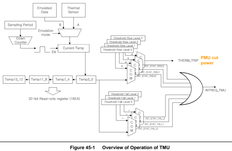
TMU monitors temperature variation in a chip by measuring on-chip temperature, and generates an interrupt to CPU when temperature exceeds or goes below pre-defined threshold. At the CPU's side, the CPU can obtain on-chip temperature information by reading the related register field.
When temperature exceeds an extremely high threshold temperature denoted as THRES_LEVEL_RISE3 field of THRESHOLD_TEMP_RISE register, then S5P6818 should not be damaged by the hot temperature. In this case, TMU urgently sends an active-high signal (THERM_TRIP) to PMU, and thermal tripping by hardware logic i.e PMU (Power Management Unit) is performed. Thermal tripping means that PMU cut off the whole power of S5P6818 by controlling external voltage regulator
tmuctrl_0: tmuctrl@c0096000 {
compatible = "nexell,s5p6818-tmu";
reg = <PHYS_BASE_TMU0 0x100>;
interrupts = <0 IRQ_TMU0 0>;
clocks = <&pclk>;
clock-names = "tmu_apbif";
#include "s5p6818-tmu-sensor-conf.dtsi"
<--
#thermal-sensor-cells = <0>; This TMU will be used as a thermal sensor under Linux’s Thermal Framework. see board DTS
further below for more info.
samsung,tmu_gain = <5>;
samsung,tmu_reference_voltage = <16>;
samsung,tmu_noise_cancel_mode = <4>;
samsung,tmu_efuse_value = <0x5d2d>;
samsung,tmu_min_efuse_value = <16>;
samsung,tmu_max_efuse_value = <76>;
samsung,tmu_first_point_trim = <25>;
samsung,tmu_second_point_trim = <85>;
samsung,tmu_default_temp_offset = <25>;
samsung,tmu_cal_type = <TYPE_ONE_POINT_TRIMMING>;
-->
soc,tieoff = <NX_TIEOFF_Inst_TMU0_SENSING_START 1>;
status = "disabled";
};
tmuctrl_1: tmuctrl@c0097000 {
compatible = "nexell,s5p6818-tmu";
reg = <PHYS_BASE_TMU1 0x100>;
interrupts = <0 IRQ_TMU1 0>;
clocks = <&pclk>;
clock-names = "tmu_apbif";
#include "s5p6818-tmu-sensor-conf.dtsi"
<--
#thermal-sensor-cells = <0>; This TMU will be used as a thermal sensor under Linux’s Thermal Framework. see board DTS
further below for more info.
samsung,tmu_gain = <5>;
samsung,tmu_reference_voltage = <16>;
samsung,tmu_noise_cancel_mode = <4>;
samsung,tmu_efuse_value = <0x5d2d>;
samsung,tmu_min_efuse_value = <16>;
samsung,tmu_max_efuse_value = <76>;
samsung,tmu_first_point_trim = <25>;
samsung,tmu_second_point_trim = <85>;
samsung,tmu_default_temp_offset = <25>;
samsung,tmu_cal_type = <TYPE_ONE_POINT_TRIMMING>;
-->
soc,tieoff = <NX_TIEOFF_Inst_TMU1_SENSING_START 1>;
status = "disabled";
};
MIPI Camera Serial Interface (CSI):
The S5P6818 has one MIPI-CSI slave.
Support YUV422 of 8 bits only.
mipi_csi:mipi_csi@c00d0000 {
compatible = "nexell,mipi_csi";
reg = <PHYS_BASE_MIPI 0x1000>;
clock-names = "mipi";
clocks = <&mipi>;
reset-names = "mipi-reset", "mipi_csi-reset", "mipi_phy_s-reset";
resets = <&nexell_reset RESET_ID_MIPI>,
<&nexell_reset RESET_ID_MIPI_CSI>,
<&nexell_reset RESET_ID_MIPI_PHY_S>;
soc,tieoff = <NX_TIEOFF_MIPI0_NX_DPSRAM_1R1W_EMAA 3>;
data_lane = <2>; camera sensor to mipi-csi data lane total number(1 ~ 4)
swap_clocklane = <0>;
swap_datalane = <0>;
pllval = <750>; 750(750MHz) or 1000(1GHz). Internally used pll value
status = "disabled";
};
Video Input Processor (VIP):
The VIP of the S5P6818 can receive images directly from external camera modules or video decoders.
It can clip or scale down the input images and store them to the memory.
The images stored from the VIP can be used for encoding by using MPEG Hardware, and as preview images by using the Multi-Layer Controller (MLC).
The images can be converted to texture images for the 3D Graphics Accelerator by using the Color Space Converter.
The S5P6818 has 3 VIP cores.
Only VIP0 can have MIPI CSI input.
vip_0:vip@c0063000 {
compatible = "nexell,vip";
reg = <PHYS_BASE_VIP0 0x1000>;
interrupts = <0 IRQ_VIP0 0>;
clock-names = "vip0";
clocks = <&vip0>;
reset-names = "vip0-reset";
resets = <&nexell_reset RESET_ID_VIP0>;
module = <0>;
status = "disabled";
};
vip_1:vip@c0064000 {
compatible = "nexell,vip";
reg = <PHYS_BASE_VIP1 0x1000>;
interrupts = <0 IRQ_VIP1 0>;
clock-names = "vip1";
clocks = <&vip1>;
reset-names = "vip1-reset";
resets = <&nexell_reset RESET_ID_VIP1>;
module = <1>;
status = "disabled";
};
vip_2:vip@c0099000 {
compatible = "nexell,vip";
reg = <PHYS_BASE_VIP2 0x1000>;
interrupts = <0 IRQ_VIP2 0>;
clock-names = "vip2";
clocks = <&vip2>;
reset-names = "vip2-reset";
resets = <&nexell_reset RESET_ID_VIP2>;
module = <2>;
status = "disabled";
};
Each VIP core has its own clipper.
A clipper clip vip input data and give data to the decimator and save clipped data to memory.
clipper_0:clipper0@c0063000 {
compatible = "nexell,nx-clipper";
module = <0>;
status = "disabled";
};
clipper_1:clipper1@c0064000 {
compatible = "nexell,nx-clipper";
module = <1>;
status = "disabled";
};
clipper_2:clipper2@c0064000 {
compatible = "nexell,nx-clipper";
module = <2>;
status = "disabled";
};
Each VIP core has its own decimator.
Decimator can scale down input images and save them to memory.
decimator_0:decimator0@c0063000 {
compatible = "nexell,nx-decimator";
module = <0>;
status = "disabled";
};
decimator_1:decimator1@c0064000 {
compatible = "nexell,nx-decimator";
module = <1>;
status = "disabled";
};
decimator_2:decimator2@c0099000 {
compatible = "nexell,nx-decimator";
module = <2>;
status = "disabled";
};
Nexell Rear Camera Driver:
This is to operate the camera as quickly as possible and start outputting on rear gear operation. (action detected using gpio).
See board DTS for complete definition.
rearcam: rear_camera {
compatible = "nexell,nx-rearcam";
interrupts = <0 IRQ_VIP0 0>, <0 IRQ_VIP1 0>, <0 IRQ_VIP2 0>; rear camera uses all main VIPs interrupts
interrupts-names = "vip.0", "vip.1", "vip.2";
status = "disabled";
};
Display Controller:
The S5P6818 has the following display features:
- 2 Multi-layer Controller, 2 Display Controller
- 1 HDMI, 1 LVDS, 1 MIPI DSI
- Supports TFT/MPU LCD Interface, HDMI(Progressive/Interlace), LVDS, MIPI DSI, NTSC/PAL output formats
- Supports transmitting the same image through different outputs at the same time.
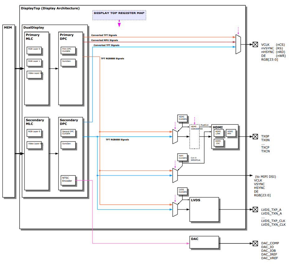
Display Controller:
The Display controller is a block that generates the signals to interface with external display devices, such as a TFT-LCD, or video encoder.
The DPC consists of a Sync generator.
The Sync generator transmits control signals (VSYNC & FIELD) to the Multi-Layer Controller (MLC) and receives RGB data from the MLC. Then the Sync generator converts the received RGB data into a suitable format.
The Sync generator can support various types of LCD and video encoders adjusting various output formats and Sync signals.
The main control signals are:
- HSync (Horizontal Sync): This signal indicates the start of a new horizontal line on a display device. It is a pulse signal that is generated at the end of each line and indicates to the display device when to reset the position of its electron beam to the beginning of the next line.
- VSync (Vertical Sync): This signal indicates the start of a new frame on a display device. It is a pulse signal that is generated at the end of each frame and indicates to the display device when to reset the position of its electron beam to the beginning of the next frame.
- FIELD: In interlaced video, a frame is divided into two fields, each containing alternating lines of the image. The Field signal indicates which field is being displayed at a given time. It is a pulse signal that is generated at the start of each field and alternates between fields for each frame. The Field signal is used to synchronize the display device with the incoming video signal and ensure that the fields are displayed in the correct order.
Ex:
In a 1080i video signal, each frame can be made up of two fields of 540 horizontal lines each. The first field contains the odd-numbered lines (1, 3, 5, etc.) and the second field contains the even-numbered lines (2, 4, 6, etc.). The Field signal would indicate which of these two fields is currently being displayed on the screen.
By interlacing the frames, where each frame is split into two fields containing alternating lines, the display device can show a complete image at a lower frame rate, but with less noticeable flicker. The alternating fields effectively double the perceived refresh rate, which can help to reduce flicker and improve the overall quality of the image.
See deinterlace block below for more info.
Multi-layer Controller:
The Multi Layer Controller of S5P6818 reads and compounds various screen components (RGB pictures, moving pictures, etc) in terms of Hardware, to organize a desired screen and transmits the result to the display controller.
Features:
- Dual register-set architecture
- Two/One RGB layers and one Video layer (Primary Display: 2 RGB layer, Secondary Display: 1 RGB layer )
- RGB layers can be used as 3D layers.
- Various pixel formats
- RGB layer: RGB/BGR 332, 444, 555, 565, 888 with/without Alpha
- Video layer: 2D Separated YUV 4:4:4, 4:2:2, 4:2:0, Linear YUV 4:2:2(YUYV)
- Various blending effects between layers : Per-layer or Per-pixel Alpha blending, Transparency, Inverse color
- Free layer position and size in pixel units
- Hardware clipping
- Vertical flip
- Video layer priority
- Gamma Correction
- Configurable Burst Length (LOCKSIZE, RGB layer)
- Scale-up/down (Video layer only) : Bilinear interpolation, Nearest neighbor sampling scale-up/down
- Color control (Video layer only) : Brightness, Contrast, Hue, Saturation
dp_drm: display_drm {
compatible = "nexell,s5pxx18-drm";
reg = <0xc0102800 0x100>, <0xc0102c00 0x100>,
<0xc0102000 0x100>, <0xc0102400 0x100>; on the way, we control the MLC too.
reg-names = "dpc.0", "dpc.1", "mlc.0", "mlc.1";
interrupts = < 0 IRQ_DPC_P 0 >, <0 IRQ_DPC_S 0>; Each DPC (primary and secondary) can generate an interrupt whenever a VSYNC occurs.
interrupts-names = "dpc.0", "dpc.1";
resets = <&nexell_reset RESET_ID_DISPLAY>,
<&nexell_reset RESET_ID_DISP_TOP>;
reset-names = "rsc-display", "rsc-display-top";
status = "disabled";
ports {
#address-cells = <1>;
#size-cells = <0>;
port@0 { }; primary DPC
port@1 { }; secondary DPC
};
};
RGB lcd-panel display:
dp_drm_rgb: display_drm_rgb {
compatible = "nexell,s5pxx18-drm-rgb";
reg = <0xc0101000 0x100>; base addr corresponds to the output DPC Muxes i.e., configure which DPC to use for output for this display.
resets = <&nexell_reset RESET_ID_DISP_TOP>;
reset-names = "rsc-display-top";
#address-cells = <1>;
#size-cells = <0>;
status = "disabled";
};
LVDS display:
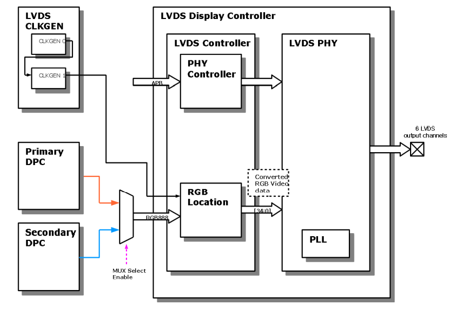
dp_drm_lvds: display_drm_lvds {
compatible = "nexell,s5pxx18-drm-lvds";
reg = <0xc0101000 0x100>; base addr corresponds to the output DPC Muxes i.e., configure which DPC to use for output for this display.
resets = <&nexell_reset RESET_ID_DISP_TOP>;
reset-names = "rsc-display-top";
#address-cells = <1>;
#size-cells = <0>;
status = "disabled";
dp-resource { sub node to config display port.
reg_base = <0xc010a000 0x100>; base addr for LVDS control regs
clk_base = <0xc0108000 3>;
resets = <&nexell_reset RESET_ID_LVDS>;
reset-names = "rsc-lvds-phy";
};
};
MIPI DSI display:
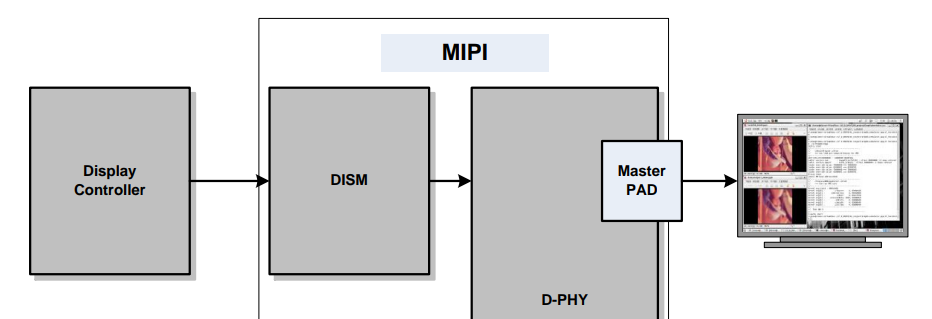
dp_drm_mipi: display_drm_mipi {
compatible = "nexell,s5pxx18-drm-mipi";
reg = <0xc0101000 0x100>;
resets = <&nexell_reset RESET_ID_DISP_TOP>;
reset-names = "rsc-display-top";
#address-cells = <1>;
#size-cells = <0>;
status = "disabled";
dp-resource {sub node to config display port.
reg_base = <0xc00d0000 0x100>;
clk_base = <0xc0105000 2>;
resets = <&nexell_reset RESET_ID_MIPI>,
<&nexell_reset RESET_ID_MIPI_DSI>,
<&nexell_reset RESET_ID_MIPI_PHY_S>,
<&nexell_reset RESET_ID_MIPI_PHY_M>;
reset-names = "rsc-mipi", "rsc-mipi-dsi",
"rsc-mipi-phy-s", "rsc-mipi-phy-m";
soc,tieoff = <NX_TIEOFF_MIPI0_NX_DPSRAM_1R1W_EMAA 3>,
<NX_TIEOFF_MIPI0_NX_DPSRAM_1R1W_EMAB 3>;
};
};
HDMI display:
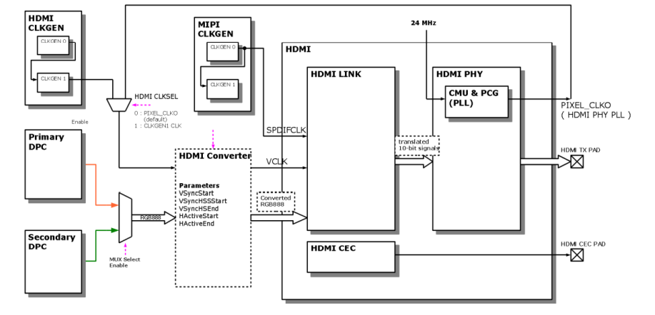
dp_drm_hdmi: display_drm_hdmi{
compatible = "nexell,s5pxx18-drm-hdmi";
reg = <0xc0101000 0x100>;
interrupts = < 0 IRQ_HDMI 0 >; interrupt for the HPD signal (Hot Plug Detect)
resets = <&nexell_reset RESET_ID_DISP_TOP>;
reset-names = "rsc-display-top";
#address-cells = <1>;
#size-cells = <0>;
status = "disabled";
dp-resource {sub node to config display port.
reg_base = <0xc0000000 0x300000>;
clk_base = <0xc0109000 4>, <0xc0105000 2>;
resets = <&nexell_reset RESET_ID_HDMI_VIDEO>,
<&nexell_reset RESET_ID_HDMI_SPDIF>,
<&nexell_reset RESET_ID_HDMI_TMDS>,
<&nexell_reset RESET_ID_HDMI>,
<&nexell_reset RESET_ID_HDMI_PHY>;
reset-names = "rsc-hdmi-video", "rsc-hdmi-spdif",
"rsc-hdmi-tmds", "rsc-hdmi", "rsc-hdmi-phy";
soc,tieoff = <NX_TIEOFF_DISPLAYTOP0_i_HDMI_PHY_REFCLK_SEL 1>;
};
};
Analogue TV OUT Display:
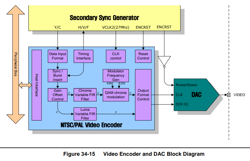
dp_drm_tvout: display_drm_tv {
compatible = "nexell,s5pxx18-drm-tv";
reg = <0xc0101000 0x100>;
resets = <&nexell_reset RESET_ID_DISP_TOP>;
reset-names = "rsc-display-top";
#address-cells = <1>;
#size-cells = <0>;
status = "disabled";
crtc-pipe = <1>;
crtcs-possible-mask = <2>;
dp-resource {
reg_base = <0xc0000000 0x300000>;
clk_base = <0xc0109000 4>;
resets = <&nexell_reset RESET_ID_HDMI_VIDEO>,
<&nexell_reset RESET_ID_HDMI_SPDIF>,
<&nexell_reset RESET_ID_HDMI_TMDS>,
<&nexell_reset RESET_ID_HDMI>,
<&nexell_reset RESET_ID_HDMI_PHY>;
reset-names = "rsc-hdmi-video",
"rsc-hdmi-spdif",
"rsc-hdmi-tmds",
"rsc-hdmi",
"rsc-hdmi-phy";
soc,tieoff = <NX_TIEOFF_DISPLAYTOP0_i_HDMI_PHY_REFCLK_SEL 1>;
};
};
Multi-Format Video Codec (Video Processing Unit / VPU):
This is a CODA960 full HD multi-standard video IP for consumer multimedia products such as HDTVs, HD set-top boxes, and HD DVD players. It can decode compressed video in a format of H.264 BP/MP/HP, VC-1 SP/MP/AP, MPEG-1/2, MPEG-4 SP/ASP, H.263P3, VP8,Theora, AVS, RV8/9/10, and JPEG (max. 8192 8192) It can also perform H.264, MPEG-4, and H.263 encoding up to Full-HD 1920 1088 (max. 8192 8192 JPEG) resolution.
The VPU can perform simultaneous multiple real time encoding, decoding, or both encoding and decoding of different format video streams at multiple resolutions.
The VPU contains a 16-bit DSP called BIT processor that controls the sub-blocks of the VPU with minimum intervention of the CPU.
video-codec@c0080000 {
compatible = "nexell, nx-vpu"; there is a space after ‘,’ ! it simply means that this driver will not be probed :)
reg = <0xc0080000 0x4000>;
interrupts = <0 IRQ_CODA960_HOST 0>,
<0 IRQ_CODA960_JPG 0>;
resets = <&nexell_reset RESET_ID_CODA_A>,
<&nexell_reset RESET_ID_CODA_P>,
<&nexell_reset RESET_ID_CODA_C>;
reset-names = "vpu-a-reset", "vpu-p-reset",
"vpu-c-reset";
clocks = <&pclk>, <&bclk>;
status = "okay";
sram = <0 0>; To enable SRAM, should set to <0xFFFF0000 0x8000> (base_address size)
};
Real Time Clock (RTC):
The RTC block is composed of 32-bit free counter register and works with an external 32.768 kHz Crystal and have the following features:
- 32-bit Counter
- Alarm Function: Alarm Interrupt or Wake Up from Power Down Mode
- Independent power pin (VDD_RTC)
- Supports 1 Hz Time interrupt for Power Down Mode
- Generates Power Management Reset signal
rtc@c0010c00 {
compatible = "nexell,nx-rtc";
reg = <PHYS_BASE_RTC 0x100>, <0xc0010200 0x100>;
interrupts = <0 IRQ_RTC 0>;
status = "disabled";
};
Scaler Controller:
The Scaler is the block used to change image size. The Scaler reads an image from the memory and writes the image to the memory after Up/Down Scaling and Low-pass Filtering. The Scaler also has the Flip and Rotation functions.
scaler@c0066000 {
compatible = "nexell,scaler";
reg = <PHYS_BASE_SCALER 0x1000>;
interrupts = <0 IRQ_SCALER 0>;
clock-names = "scaler";
clocks = <&scaler>;
reset-names = "scaler-reset";
resets = <&nexell_reset RESET_ID_SCALER>;
status = "disabled";
};
3D Graphic Engine (GPU):
S5P6818 has a powerful 3D GPU engine. 3D GPU is a hardware accelerator for 2D and 3D graphics systems. The GPU consists of:
- 2 Pixel Processors (PPs)
- 1 Geometry Processor (GP)
- A 32 Kbyte Level 2 Cache (L2)
- A Memory Management Unit (MMU) for each GP and PP
- A Power Management Unit (PMU).
Compatible with OpenGL ES 2.0 OpenGL ES 1.1 OpenVG 1.1.
From the description above this is a MALI400MP2 ARM GPU, however from the number of interrupts below, this is a MALI400MP4 ARM GPU !!!!!!!!!!
gpu@c0070000 {
compatible = "arm,mali-400", "arm,mali-utgard";
reg = <PHYS_BASE_VR 0x10000>; Zero info in datasheet for GPU regs !
interrupts = <0 IRQ_VR 0>, <0 IRQ_VR 0>, <0 IRQ_VR 0>,
<0 IRQ_VR 0>, <0 IRQ_VR 0>, <0 IRQ_VR 0>,
<0 IRQ_VR 0>, <0 IRQ_VR 0>, <0 IRQ_VR 0>,
<0 IRQ_VR 0>, <0 IRQ_VR 0>;
interrupt-names = "IRQGP", "IRQGPMMU", "IRQPP0",
"IRQPPMMU0", "IRQPP1", "IRQPPMMU1",
"IRQPP2", "IRQPPMMU2", "IRQPP3",
"IRQPPMMU3", "IRQPMU";
pmu_domain_config = <0x1 0x4 0x8 0x10 0x20 0x0 0x0 0x0
0x0 0x2 0x0 0x0>;
pmu_switch_delay = <0xff>;
clocks = <&vr>;
clock-names = "clk_mali";
resets = <&nexell_reset RESET_ID_VR>;
reset-names = "vr-reset";
};
Deinterlace Block:
This is a memory to memory device.
What is interlacing ?
An interlaced video frame consists of two fields taken in sequence: the first containing all the odd lines of the image, and the second all the even lines. Analog television employed this technique because it allowed for less transmission bandwidth while keeping a high frame rate for smoother and more life-like motion. Interlacing enhances motion perception to the viewer, and reduces flicker by taking advantage of the phi phenomenon and analog TVs nature..
What is deinterlacing ?
Most modern displays, such as LCD, DLP and plasma displays, are not able to work in interlaced mode (the interlacing becomes noticeable and can appear as a distracting visual defect), because they are fixed-resolution displays and only support progressive scanning. In order to display interlaced signals on such displays, the two interlaced fields must be converted to one progressive frame with a process known as de-interlacing.
When displaying an interlaced frame, the FIELD sync signal is used to know which lines of the frame are currently displayed i.e., odd or even lines.
This means that at any moment, we never display the whole frame at once, only odd or even lines of the frame are displayed.
This is where the deinterlacer comes in ! The deinterlacer gives the possibility to display a whole frame again, even if we have only odd or even lines of the original frame.
The deinterlacer calculates the missing lines and completes the frame data. In other words, if we currently have only the odd lines of a frame, the deinterlacer will calculate the value of the even lines using a specific algorithm. The same happens if we currently have only the even lines. (see TRM for more info)
deinterlacer: deinterlacer@c0065000 {
compatible = "nexell,nx-deinterlacer";
reg = <PHYS_BASE_DEINTERLACE 0x1000>;
interrupts = <0 IRQ_DEINTERLACE 0>;
clock-names = "deinterlace";
clocks = <&deinterlace>;
reset-names = "deinterlace-reset";
resets = <&nexell_reset RESET_ID_DEINTERLACE>;
status = "disabled";
};
}; /*** soc ***/
};
####################################################################################################################################
#### Board DTS
####################################################################################################################################
/*
* Copyright (C) 2016 Nexell Co., Ltd.
* Author: Hyejung Kown <cjscld15@nexell.co.kr>
*
* This program is free software; you can redistribute it and/or
* modify it under the terms of the GNU General Public License
* as published by the Free Software Foundation; either version 2
* of the License, or (at your option) any later version.
*
* This program is distributed in the hope that it will be useful,
* but WITHOUT ANY WARRANTY; without even the implied warranty of
* MERCHANTABILITY or FITNESS FOR A PARTICULAR PURPOSE. See the
* GNU General Public License for more details.
*
* You should have received a copy of the GNU General Public License
* along with this program. If not, see <http://www.gnu.org/licenses/>.
*/
#include <dt-bindings/interrupt-controller/irq.h>
#include <dt-bindings/gpio/gpio.h>
#include <dt-bindings/input/input.h>
#include "s5p6818.dtsi"
#include "../../../../../include/generated/autoconf.h"
/ {
S5P6818 memory map: up to 2GBytes of DDR3
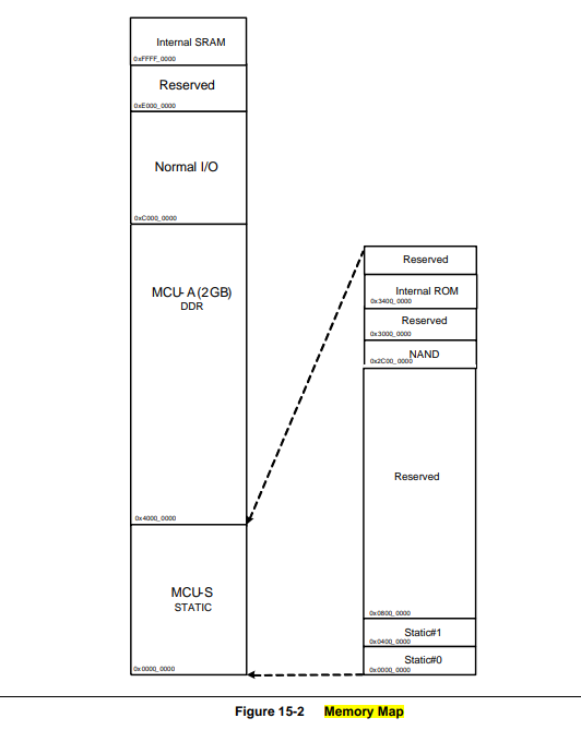
memory {
device_type = "memory";
reg = <0x40000000 0x7db00000>; 1.96 Gbytes of DDR memory. (the rest could be reserved for optee for example)
};
aliases {
i2c1 = &i2c_gpio1;
i2c3 = &i2c_gpio3;
i2c5 = &i2c_gpio5;
i2c6 = &i2c_gpio6;
i2c7 = &i2c_gpio7;
};
nx-v4l2 {
status = "okay";
};
soc {
#include "s5p6818-pinctrl.dtsi"
clocks { change some clk freqs
uart3:uart@c00ab000 { clock-frequency = <147500000>; };
i2c2:i2c@c00b0000 { clock-frequency = <200000000>; };
pwm0:pwm0@c00ba000 {
clk-input = <I_PLL2>;
clock-frequency = <10000000>;
};
pwm1:pwm1@c00ba000 {
clk-input = <I_PLL2>;
clock-frequency = <10000000>;
};
pwm2:pwm2@c00be000 {
clk-input = <I_PLL2>;
clock-frequency = <10000000>;
};
pwm3:pwm3@c00be000 {
clk-input = <I_PLL2>;
clock-frequency = <10000000>;
};
};
dynamic-freq@bb000 {define supply used for DVFS
supply_name = "vdd_core_regulator";
vdd_core_regulator-supply = <&VCC_DCDC0>;
};
serial0:serial@c00a1000 {use dma for uart transfers
dmas = <&pl08xdma0 2>, <&pl08xdma0 3>;
dma-names = "tx", "rx";
status ="okay";
};
serial1:serial@c00a0000 {
dmas = <&pl08xdma0 0>, <&pl08xdma0 1>;
dma-names = "tx", "rx";
status ="okay";
};
serial2:serial@c00a2000 {
dmas = <&pl08xdma0 4>, <&pl08xdma0 5>;
dma-names = "tx", "rx";
status ="okay";
};
serial3:serial@c00a3000 {
status ="okay";
};
serial4:serial@c006d000 {
status ="okay";
};
amba {
pl08xdma0:pl08xdma@c0000000 {
use_isr; use ISRs instead of tasklets for interrupt callbacks
};
pl08xdma1:pl08xdma@c0001000 {
use_isr; use ISRs instead of tasklets for interrupt callbacks
};
};
dw_mmc_2:dw_mmc@c0069000 { define main board emmc characteristics
num-slots = <1>;
bus-width = <8>;
mmc-ddr-1_8v;
pinctrl-0 = <&sdmmc2_cclk &sdmmc2_cmd
&sdmmc2_bus4 &sdmmc2_bus8>;
soc,tieoff = <NX_TIEOFF_MMC_8BIT 1>;
cap-mmc-highspeed; Enables support for high speed cards (up to 50MHz)
broken-cd; no cd for emmc
non-removable; embedded mmc
clock-frequency = <200000000>;
card-detect-delay = <200>; Delay in milli-seconds before detecting card after card insert event
disable-wp; no write protect
status = "okay";
nexell,drive_dly = <0x0>; Output drive clock delay. range is 0 ~ 255.
nexell,drive_shift = <0x03>; Output drive clock phase shift. range is 0 ~ 3
nexell,sample_dly = <0x00>; Read sample clock delay. range is 0 ~ 255.
nexell,sample_shift = <0x02>; Read sample clock phase shitf. range is 0 ~ 255.
};
dw_mmc_0:dw_mmc@c0062000 { define sd-mmc port characteristics
num-slots = <1>;
bus-width = <4>;
cap-sd-highspeed; Enables support for high speed cards (up to 50MHz)
clock-frequency = <100000000>;
card-detect-delay = <200>;
disable-wp;
cd-gpios = <&gpio_e 31 0>; card detect pin
cd-inverted;
nexell,drive_dly = <0x0>;
nexell,drive_shift = <0x02>;
nexell,sample_dly = <0x00>;
nexell,sample_shift = <0x01>;
status = "okay";
};
tmuctrl_0: tmuctrl@c0096000 {
status = "okay";
};
Thermal Framework Device Tree descriptor:
https://www.kernel.org/doc/Documentation/devicetree/bindings/thermal/thermal.txt
The objective of device tree thermal descriptors is to describe only the hardware thermal aspects. The thermal device tree bindings are not about how the system must control or which algorithm or policy must be taken in place.
There are five types of nodes involved to describe thermal bindings:
- thermal sensors: devices which may be used to take temperature measurements.
- cooling devices: devices which may be used to dissipate heat.
- trip points: describe key temperatures at which cooling is recommended. The set of points should be chosen based on hardware limits.
- cooling maps: used to describe links between trip points and cooling devices;
- thermal zones: used to describe thermal data within the hardware;
Thermal sensor devices:
Thermal sensor devices are nodes providing temperature sensing capabilities on thermal zones.
Required property:
- #thermal-sensor-cells: Used to provide sensor device specific information while referring to it. Typically 0 on thermal sensor nodes with only one sensor, and at least 1 on nodes with several internal sensors, in order to uniquely identify the sensor instances within the IC.
Cooling device nodes:
Cooling devices are nodes providing control on power dissipation. There are essentially two ways to provide control on power dissipation. First is by means of regulating device performance, which is known as passive cooling. A typical passive cooling is a CPU that has dynamic voltage and frequency scaling (DVFS), and uses lower frequencies as cooling states. Second is by means of activating devices in order to remove the dissipated heat, which is known as active cooling, e.g. regulating fan speeds.
Required property:
- #cooling-cells: Used to provide cooling device specific information while referring to it. Must be at least 2, in order to specify minimum and maximum cooling state used in the reference.
Trip points:
The trip node is a node to describe a point in the temperature domain in which the system takes an action. This node describes just the point, not the action.
Required properties:
- temperature: An integer indicating the trip temperature level, in millicelsius.
- hysteresis: A low hysteresis value on temperature property (above). This is a relative value, in millicelsius.
- type: a string containing the trip type. Expected values are:
"active": A trip point to enable active cooling
"passive": A trip point to enable passive cooling
"hot": A trip point to notify emergency
"critical" Hardware not reliable.
Cooling maps:
The cooling-maps is a node to describe how cooling devices get assigned to trip points of the zone.
Required properties:
- cooling-device: A list of phandles of cooling devices with their specifiers, referring to which cooling devices are used in this binding. In the cooling specifier, the first cell is the minimum cooling state and the second cell is the maximum cooling state used in this map.
- trip: A phandle of a trip point node within the same thermal zone.
thermal-zones {
cpu0_thermal: cpu0-thermal {
thermal-sensors = <&tmuctrl_0>; the tmuctrl_0 is considered as a thermal sensor device.
polling-delay-passive = <1000>; The maximum number of milliseconds to wait between polls when performing passive cooling.
polling-delay = <1000>; The maximum number of milliseconds to wait between polls when checking this thermal zone
trips {
cpu_alert0: cpu-alert-0 {
temperature = <80000>; alert0 at 80°C
hysteresis = <0>;
type = "active"; This is not correct ! it must be passive as it is linked to the CPU in cooling maps (active cooling is
for fans)
};
cpu_alert1: cpu-alert1 {
temperature = <85000>;alert1 at 85°C
hysteresis = <0>;
type = "active";This is not correct ! it must be passive as it is linked to the CPU in cooling maps (active cooling is
for fans)
};
cpu-crit-0 {
temperature = <115000>;critical temperature at 115°C
hysteresis = <0>;
type = "critical"; HW is no more reliable at his temperature
};
};
cooling-maps {
map0 { when CPU reaches 80°C, start active passive cooling from level0 till 9th level
trip = <&cpu_alert0>;
cooling-device = <&cpu0 0 9>;
};
map1 { if CPU reaches 85°C, continue active passive cooling till level10 and don’t go below the 9th level
trip = <&cpu_alert1>;
cooling-device = <&cpu0 9 10>;
};
};
};
};
spdif_tx: spdiftx@c0059000 {
#sound-dai-cells = <1>; This is specified to link this DAI (Digital Audio Interface) to Linux’s simple sound card framework. for more info see the
“sound” node below.
The value should be 0 not 1, as the SPDIF-Tx has only one data channel.
pcm-bit = <16>; Select PCM (Pulse Code Modulation) sampling bit size. (16/24 bits)
sample_rate = <48000>; Select sample rate. (44100~96000 hz)
status = "okay";
};
watchdog@c0019000 {
status = "okay";
};
rtc@c0010c00 {
status = "okay";
};
nexell_usbphy: nexell-usbphy@c0012000 {
status = "okay";
};
ehci@c0030000 {
status = "okay";
port@0 {
status = "okay"; enable usb2.0 host
};
};
ohci@c0020000 {
status = "okay";
port@0 {
status = "okay"; enable usb1.1 host
};
};
dwc2otg@c0040000 {
gpios = <&alive_0 5 0>; specify the pin used for USB_OTG_ID i.e. to set default OTG mode: high->controller is peripheral,
low-> controller is host. The last 0 is for GPIO_ACTIVE_HIGH i.e., vcc=high and gnd=low
status = "okay";
};
pwm:pwm@c0018000 {
clock-names = "timers", "pwm-tclk0", "pwm-tclk1";
clocks = <&pclk>, <&pwm0>, <&pwm2>;
pinctrl-names = "default";
pinctrl-0 = <&pwm0_pin &pwm1_pin>;
samsung,pwm-outputs = <0>, <1>;
status = "okay";
};
i2s_0:i2s@c0055000 {
#sound-dai-cells = <1>;This is specified to link this DAI (Digital Audio Interface) to Linux’s simple sound card framework. for more info see the
“sound” node below.
master-mode = <1>;
mclk-in = <0>;
trans-mode = <0>;
frame-bit = <32>;
sample-rate = <48000>;
pre-supply-mclk = <1>;
status = "okay";
};
i2s_1:i2s@c0056000 {
#sound-dai-cells = <1>;This is specified to link this DAI (Digital Audio Interface) to Linux’s simple sound card framework. for more info see the
“sound” node below.
master-mode = <1>;
mclk-in = <0>;
trans-mode = <0>;
frame-bit = <32>;
sample-rate = <48000>;
pre-supply-mclk = <1>;
status = "okay";
};
pinctrl@C0010000 { pincontrol for board pins
key_power:key_power {
nexell,pins = "alive-0";
nexell,pin-function = <0>;
nexell,pin-pull = <1>;
nexell,pin-strength = <0>;
};
key_back:key_back {
nexell,pins = "alive-1";
nexell,pin-function = <0>;
nexell,pin-pull = <1>;
nexell,pin-strength = <0>;
};
key_homepage:key_homepage {
nexell,pins = "alive-4";
nexell,pin-function = <0>;
nexell,pin-pull = <1>;
nexell,pin-strength = <0>;
};
toutchpanel_irq: touchpanel-irq {
nexell,pins = "gpiod-8";
nexell,pin-function = <0>;
nexell,pin-pull = <1>;
nexell,pin-strength = <0>;
};
};
scaler@c0066000 {
status = "okay";
};
}; /*** soc ***/
All the blow regulators are used for powering the audio SOC ALC/RT5640
vcc_spk: regulator-fix@2 {
compatible = "regulator-fixed"; Fixed Voltage regulator
regulator-name = "SPK Vcc";
regulator-min-microvolt = <5000000>; Minimum voltage output of regulator
regulator-max-microvolt = <5000000>; Maximum voltage output of regulator. a fixed voltage regulator is expected to have the
regulator-min-microvolt and regulator-max-microvolt to be the same.
regulator-boot-on; Enable regulator at boot time
regulator-always-on; Keep regulator on at all times
gpio = <&gpio_d 3 GPIO_ACTIVE_HIGH>; GPIO pin used to enable/disable regulator
enable-active-high; Enable regulator when GPIO is high
};
vdd_a: regulator-fix@3 {
compatible = "regulator-fixed";
regulator-name = "A Vdd";
regulator-min-microvolt = <1800000>;
regulator-max-microvolt = <1800000>;
regulator-boot-on;
regulator-always-on;
gpio = <&gpio_e 17 GPIO_ACTIVE_HIGH>;
enable-active-high;
};
vdd_db: regulator-fix@4 {
compatible = "regulator-fixed";
regulator-name = "DB Vdd";
regulator-min-microvolt = <3300000>;
regulator-max-microvolt = <3300000>;
regulator-boot-on;
regulator-always-on;
gpio = <&gpio_e 20 GPIO_ACTIVE_HIGH>;
enable-active-high;
};
vcc_monoamp: regulator-fix@5 {
compatible = "regulator-fixed";
regulator-name = "MONOAMP Vcc";
regulator-min-microvolt = <5000000>;
regulator-max-microvolt = <5000000>;
regulator-boot-on;
regulator-always-on;
gpio = <&gpio_d 24 GPIO_ACTIVE_HIGH>;
enable-active-high;
};
amp2_en: regulator-fix@6 {
compatible = "regulator-fixed";
regulator-name = "AMP2 EN";
regulator-min-microvolt = <5000000>;
regulator-max-microvolt = <5000000>;
regulator-boot-on;
regulator-always-on;
gpio = <&gpio_d 25 GPIO_ACTIVE_HIGH>;
enable-active-high;
};
I2C-GPIO:
https://www.kernel.org/doc/Documentation/gpio/drivers-on-gpio.txt
In Linux, standard kernel drivers exist for common GPIO tasks. These drivers provide the right in-kernel and userspace APIs/ABIs for the job, and they can quite easily interconnect with other kernel subsystems.
The following nodes use the i2c-gpio subsystem (drivers/i2c/busses/i2c-gpio.c). i2c-gpio is used to drive an I2C bus (two wires, SDA and SCL lines) by hammering (bitbang) two GPIO lines. It appears as any other I2C bus to the system and makes it possible to connect drivers for the I2C devices on the bus like any other I2C bus driver.
Required properties:
- compatible = "i2c-gpio";
- gpios: sda and scl gpio
Optional properties:
- i2c-gpio,sda-open-drain: sda as open drain
- i2c-gpio,scl-open-drain: scl as open drain
- i2c-gpio,scl-output-only: scl as output only
- i2c-gpio,delay-us: delay between GPIO operations (may depend on each platform)
- i2c-gpio,timeout-ms: timeout to get data
i2c_gpio1: i2c@1 {
compatible = "i2c-gpio";
gpios = <&gpio_d 5 0 /* sda */
&gpio_d 4 0 /* scl */>;
i2c-gpio,delay-us = <100>;
#address-cells = <1>;
#size-cells = <0>;
rt5640: rt5640@1c { ALC5640 audio CODEC
#sound-dai-cells = <0>;
compatible = "realtek,rt5640";
reg = <0x1c>; I2C addr
realtek,ldo1-en-gpios = <&gpio_c 4 GPIO_ACTIVE_HIGH>; The GPIO that controls the CODEC's LDO1_EN pin
};
};
i2c_gpio3: i2c@3 {
compatible = "i2c-gpio";
gpios = <&gpio_b 16 0 /* sda */
&gpio_b 18 0 /* scl */>;
i2c-gpio,delay-us = <100>;
#address-cells = <1>;
#size-cells = <0>;
alc5623: alc5623@1a { ALC5621/ALC5622/ALC5623 audio CODEC
#sound-dai-cells = <0>;
compatible = "realtek,alc5623";
reg = <0x1a>; I2C addr
};
};
i2c_gpio5: i2c@5 {
compatible = "i2c-gpio";
gpios = <&gpio_c 27 0 /* sda */
&gpio_c 25 0 /* scl */
>;
i2c-gpio,delay-us = <100>;
#address-cells = <1>;
#size-cells = <0>;
usb2514: usb2514@2c { USB2514 - USB 2.0 High-Speed 4-Port Hub Controller
compatible = "smsc,usb2514";
reg = <0x2c>;
reset-gpios = <&gpio_e 7 1>;
initial-mode = <1>; Should specify initial mode. (1 for HUB mode, 2 for STANDBY mode)
};
};
i2c_gpio6: i2c@6 {
compatible = "i2c-gpio";
gpios = <&gpio_d 23 0 /* sda */
&gpio_d 22 0 /* scl */
>;
i2c-gpio,delay-us = <100>;
#address-cells = <1>;
#size-cells = <0>;
};
i2c_gpio7: i2c@7 {
status = "disabled";
};
Simple Sound Card Framework:
Simple-Card specifies audio DAI (Digital Audio Interface) connections between the Soc and the Codecs on the board.
https://www.kernel.org/doc/Documentation/devicetree/bindings/sound/simple-card.txt
sound {
compatible = "nexell,simple-audio-card";
simple-audio-card,name = "s5p6818 avn_ref Audio"; User specified audio sound card name
simple-audio-card,mclk-fs = <256>; Multiplication factor between stream rate and codec master clock.
simple-audio-card,widgets = specifies audio off-codec DAPM widgets, format : "template-wname", "user-supplied-wname"
"Headphone", "Headphones",
"Microphone", "Mic Jack";
simple-audio-card,routing = A list of the connections between audio components. format : pair of strings, the first being the
connection's sink, the second is the connection's source.
"Headphones", "HPOL", HPOL, HPOR and IN1P correspond to pins in the Codec chip ! (see sound/rt5640.txt)
"Headphones", "HPOR",
"IN1P", "Mic Jack";
status = "okay";
subnode names have to be prefixed with "simple-audio-card,"
simple-audio-card,dai-link@0 { The first DAI link: i2s format, connected to i2s_0 and rt5640 codec
format = "i2s";
cpu {
sound-dai = <&i2s_0 0>; CPU DAI link
};
codec {
sound-dai = <&rt5640>; Codec DAI link
};
};
simple-audio-card,dai-link@1 { The second DAI link: i2s format, connected to i2s_1 and alc5623 codec
format = "i2s";
cpu {
sound-dai = <&i2s_1 0>;
};
codec {
sound-dai = <&alc5623>;
};
};
simple-audio-card,dai-link@2 { The third DAI link: spdif format, connected to spdif_tx and spdif_out
format = "spdif";
cpu {
sound-dai = <&spdif_tx 0>;
};
codec {
sound-dai = <&spdif_out>;
};
};
};
Dummy SPDIF transmitter for Codec DAI link.
spdif_out: spdif-out {
#sound-dai-cells = <0>;
compatible = "linux,spdif-dit";
};
GPIO-KEYS:
https://www.kernel.org/doc/Documentation/gpio/drivers-on-gpio.txt
The following node uses the gpio-keys subsystem (drivers/input/keyboard/gpio_keys.c). gpio-keys is used when your GPIO line can generate interrupts in response to a key press. It supports debounce.
Each button (key) is represented as a sub-node of "gpio-keys":
Subnode properties:
- gpios: OF device-tree gpio specification.
- interrupts: the interrupt line for that input.
- label: Descriptive name of the key.
- linux,code: Keycode to emit.
Note that either "interrupts" or "gpios" properties can be omitted, but not both at the same time. Specifying both properties is allowed.
gpio_key: gpio_keys {
compatible = "gpio-keys";
#address-cells = <1>;
#size-cells = <0>;
pinctrl-names = "default";
pinctrl-0 = <&key_power &key_back
&key_homepage>;
power {
label = "Power";
gpios = <&alive_0 0 GPIO_ACTIVE_LOW>;
linux,code = <KEY_POWER>;
gpio-key,wakeup; button can wake-up the system (deprecated in favor of ‘wakeup-source’)
};
back {
label = "Back";
gpios = <&alive_0 1 GPIO_ACTIVE_LOW>;
linux,code = <KEY_BACK>;
};
homepage {
label = "Homepage";
gpios = <&alive_0 4 GPIO_ACTIVE_LOW>;
linux,code = <KEY_HOMEPAGE>;
};
};
ION Memory Manager:
This node is specific to Android.
ION Memory Manager, used by Android to efficiently allocate buffers from userspace that can be shared between drivers.
nexell-ion@0 {
compatible = "nexell,ion";
heap_sys_user@0 {
heap-type = "ion_system";
};
heap_sys_contig@0 {
heap-type = "ion_system_contig";
};
heap_dma@0 {
heap-type = "ion_dma";
};
};
pwm-backlight bindings:
Required properties:
- compatible: "pwm-backlight"
- pwms: OF device-tree PWM specification (see PWM binding[0])
- brightness-levels: Array of distinct brightness levels. Typically these are in the range from 0 to 255, but any range starting at 0 will do. The actual brightness level (PWM duty cycle) will be interpolated from these values. 0 means a 0% duty cycle (darkest/off), while the last value in the array represents a 100% duty cycle (brightest).
- default-brightness-level: the default brightness level (index into the array defined by the "brightness-levels" property)
backlight: pwm-backlight {
compatible = "pwm-backlight";
pwms = <&pwm 0 20000 1>; use pwm channel 0, of period 20us and an inverted polarity.
pwm-names = "pwm-backlight";
brightness-levels = <30 31 32 33 34 35 36 37 38 39
40 41 42 43 44 45 46 47 48 49
50 51 52 53 54 55 56 57 58 59
60 61 62 63 64 65 66 67 68 69
70 71 72 73 74 75 76 77 78 79
80 81 82 83 84 85 86 87 88 89
90>;
default-brightness-level = <45>;
status = "okay";
};
#if defined(CONFIG_VIDEO_TW9992) Support for the Intersil/Techwell TW9900 video decoder. TW9992 is a low power NTSC/PAL analog video decoder that
is designed for automotive applications.
decimator_3:decimator3@c0063000 { this address corresponds to decimator_0 not 3 !!!!!! and decimator_0 is already defined in soc dts !!!
compatible = "nexell,nx-decimator";
module = <0>; VIP module number
logical = <1>; whether logical device or not (1 - logical, 0 or none - physical). Logical device is not a real camera device It's just for making a
logical video device to use the decimator with another sensor.
logical_num = <0>;
status = "okay";
};
clipper_3:clipper3@c0063000 {this address corresponds to clipper_0 not 3 !!!!!!
compatible = "nexell,nx-clipper";
module = <0>; VIP module number
logical = <1>; whether logical device or not (1 - logical, 0 or none - physical). Logical device is not a real camera device It's just for making a
logical video device to use the clipper with another sensor.
logical_num = <0>;
interface_type = <NX_CAPTURE_INTERFACE_MIPI_CSI>; NX_CAPTURE_INTERFACE_PARALLEL or NX_CAPTURE_INTERFACE_MIPI
gpios = <&gpio_b 23 0>; GPIO(s) to use to power up the camera sensor
data_order = <NX_VIN_CBY0CRY1>; YUV 422 data order from camera sensor
port = <1>; vip input port, each vip has two input port and can use only one
external_sync = <0>; if 1, this is 601, else 656
interlace = <1>; if 1, interlace input data
clock_source = <4>; vip clock source number. VIP can create the video in clock by using an internal PLL (clock number 3) or an external VCLK (clock
number 4) pin as a clock source.
clock_frequency = <300000000>; vip clock frequency 300MHz
status = "okay";
sensor {
type = <NX_CAPTURE_SENSOR_I2C>;
i2c_name = "tw9992"; camera sensor i2c name
i2c_adapter = <3>; adapter number
addr = <0x3d>; camera sensor i2c address
};
power {
enable_seq: camera sensor power on sequence
[ACTION_START_TAG][ACTION_TYPE][SEQUENCE][ACTION_END_TAG]
ACTION_START_TAG : NX_ACTION_START
ACTION_END_TAG : NX_ACTION_END
ACTION_TYPE : NX_ACTION_TYPE_PMIC, NX_ACTION_TYPE_GPIO, NX_ACTION_TYPE_CLOCK
SEQUENCE for ACTION_TYPE_GPIO: gpionum, value, delay_ms, value, delay_ms ...
SEQUENCE for ACTION_TYPE_PMIC: regulator_name, value, delay_ms
SEQUENCE for ACTION_TYPE_CLOCK: enable/disable, delay_ms
NOTE : gpionum is the index in the ‘gpios’ specifier defined in the root node.
enable_seq = <
NX_ACTION_START NX_ACTION_TYPE_GPIO 0 1 1 0 10 1 10 NX_ACTION_END
>;
disable_seq = < camera sensor power off sequence Action defines same to above
NX_ACTION_START NX_ACTION_TYPE_GPIO 0 0 1 NX_ACTION_END
>;
};
};
#endif
}; /* root node end */
&deinterlacer {
status = "okay";
};
&vip_0 {
clk-base = <0xc00c1000>;
status = "okay";
};
&decimator_0 {
status = "okay";
};
#if defined(CONFIG_VIDEO_TW9900)
&clipper_0 { configure clipper for TW9900 sensor (same as TW9992 above)
interface_type = <NX_CAPTURE_INTERFACE_PARALLEL>;
pinctrl-names = "default";
pinctrl-0 = <&vid0_data_clk &vid0_sync>;
gpios = <&gpio_c 9 0 &gpio_e 16 0 &gpio_e 12 0>;
data_order = <NX_VIN_CBY0CRY1>;
port = <0>;
external_sync = <0>;
interlace = <1>;
clock_source = <4>;
status = "okay";
sensor {
type = <NX_CAPTURE_SENSOR_I2C>;
i2c_name = "tw9900";
i2c_adapter = <5>;
addr = <0x44>;
};
power {
enable_seq = <
NX_ACTION_START NX_ACTION_TYPE_GPIO 2 0 1 0 10 NX_ACTION_END
NX_ACTION_START NX_ACTION_TYPE_GPIO 1 0 1 0 10 NX_ACTION_END
NX_ACTION_START NX_ACTION_TYPE_GPIO 0 1 10 NX_ACTION_END
>;
};
};
#endif
/ {
sensor_tw9900:register {
data = <0x02 0x40>, sensor initial data in the form : <reg value>
<0x1c 0x00>,
<0x03 0xa6>,
<0x06 0x80>,
<0x07 0x02>,
<0x08 0x15>,
<0x09 0xf0>,
<0x0a 0x09>,
<0x0b 0xc0>,
<0x10 0xec>,
<0x11 0x68>,
<0x19 0x50>,
<0x1b 0x00>,
<0x1a 0x0f>,
<0x2f 0xe6>,
<0x55 0x00>,
<0xaf 0x40>,
<0xb1 0x20>,
<0xb4 0x20>;
};
};
&rearcam {
rotation = <0>; the display rotation property. values: <0> - Not rotate. <1> - Rotation.
rear_cam_dev = <&clipper_0>; use clipper_0/vip0
sensor_reg = <&sensor_tw9900>; node to sensor data.
display = <&dp_drm>; link to DPC
dp_drm_dev = <&dp_drm_lvds>; DPC output node
width = <704>; the width for display image.
height = <480>; the height for display image.
skip_frame = <0>;
status = "okay";
gpio {
event-gpio = <&alive_0 3 0>; the GPIO for rear gear detection.
active_high = <0>;
detect_delay = <0>; delay of operation after rear gear detection.
};
deinterlace { useless: deinterlacer child is not supported in the rear camera driver
use = <0>;
divide_frame = <0>;
is_odd_first = <1>;
};
mlc {
module = <0>; use primary MLC
format = <0x06530000>; the MLC format for rgb display. form Table 33-5 in TRM, 0x06530000 corresponds to A8R8G8B8
};
dpc {
module = <0>; use primary DPC
};
};
&mipi_csi {
data_lane = <2>; camera sensor to mipi-csi data lane total number(1 ~ 4)
pllval = <750>; 750(750MHz) or 1000(1GHz). Internally used pll value
hssettle = <7>; value for HSSETTLE field of CSIS_DPHYCTRL
status = "okay";
};
&dp_drm {
status = "okay";
ports {
port@0 { MLC0 configuration
reg = <0>;
back_color = < 0x0 >; top layer's background color. Specifies the background color to be displayed on the screen in areas not covered by any of
the layers.
color_key = < 0x0 >; video layer's color key value
plane-names = "rgb", "primary", "video"; MLC0 has 2 RGB layers and one video layer.
};
port@1 {MLC1 configuration
reg = <1>;
back_color = < 0x0 >;
color_key = < 0x0 >; video layer's color key value
plane-names = "video", "primary"; MLC1 has only one RGB layer and and one video layer
};
};
};
&dp_drm_lvds {
status = "ok";
display-timing { set typical videomode of lcd panel
clock-frequency = <50000000>; display clock in Hz
hactive = <1024>; display resolution
vactive = <600>; display resolution
hfront-porch = <160>; horizontal display timing parameters in pixels
hback-porch = <140>;
hsync-len = <20>;
vfront-porch = <12>; vertical display timing parameters in pixels
vback-porch = <20>;
vsync-len = <3>;
};
dp_control { config display port hw parameters
clk_src_lv0 = <3>; select display clock source of clock generator '0' -> 0:PLL0, 1:PLL1, 2:SVLCK, 3:P(S)VCLK, 4:~P(S)VCLK, 5:AVCLK
6:~SVLCK, 7:ClKGEN0's Output( Only use Clock generator1 )
clk_div_lv0 = <16>; set display clock divisor of specified clock generator '0' (1 ~ 256)
clk_src_lv1 = <7>;
clk_div_lv1 = <1>;
out_format = <2>; specifies display out data format
};
};
&dp_drm_hdmi {
ddc-i2c-bus = <&i2c_gpio6>; I2C controller used for DDC EDID probing
status = "ok";
};
&i2c_2 {
#address-cells = <1>;
#size-cells = <0>;
status = "okay";
rate = <400000>;
tsc2007: tsc2007@48 { touchscreen controller
compatible = "ti,tsc2007";
gpios = <&gpio_d 8 0>; gpio connected to tsc2007 irqpin. When panel touched irqpin goes low
interrupt-parent = <&gpio_d>;
interrupts = <8 IRQ_TYPE_EDGE_FALLING>; first cell: gpio number, second cell: irq detect flag
pinctrl-names = "default";
pinctrl-0 = <&toutchpanel_irq>;
reg = <0x48>; i2c addr
ti,x-plate-ohms = <180>; X-plate resistance in ohms
};
};
#define PMIC_PDATA_INIT(_id, _rname, _minuv, \
_maxuv, _init_uv, _init_enable, \
_set_init_uV, _slp_slots) \
regulator-name = _rname; \
regulator-min-microvolt = <_minuv>; \
regulator-max-microvolt = <_maxuv>; \
nx,id = <_id>; \
nx,init_enable = <_init_enable>; \
nx,init_uV = <_init_uv>; \
nx,set_init_uV = <_set_init_uV>; \
nx,sleep_slots = <_slp_slots>;
&i2c_gpio7 {
compatible = "i2c-gpio";
gpios = <&gpio_e 8 0 /* SDA */
&gpio_e 9 0 /* SCL */
>;
#address-cells = <1>;
#size-cells = <0>;
status = "okay";
nxe2000@32 { PMIC node ! finally !
compatible = "nexell,nxe2000";
reg = <0x32>; I2C addr
interrupt-parent = <&alive_0>;
interrupts = <0x5 IRQ_TYPE_EDGE_FALLING>; PMIC irq pin connected to alive0 pin5. However, the same pin is used in dwc2otg as the
USB_OTG_ID pin !!!!!!!!!!
regulators { The NXE2000 has 5 step-down DC/DC converters and 12 low dropout regulators.
VCC_DCDC0:
dcdc1 { PMIC_PDATA_INIT( 0,
"nxe2000_dcdc1",
900000, 1500000,
1100000, 1, 0, 0x4)
regulator-always-on; Keep regulator on at all times
regulator-boot-on;}; Enable regulator at boot time
VCC_DCDC1:
dcdc2 { PMIC_PDATA_INIT( 1,
"nxe2000_dcdc2",
1000000, 1500000,
1200000, 1, 0, 0x4)
regulator-always-on;
regulator-boot-on;};
VCC_DCDC2:
dcdc3 { PMIC_PDATA_INIT( 2,
"nxe2000_dcdc3",
1000000, 3500000,
3300000, 1, 1, 0x0)
regulator-always-on;
regulator-boot-on;};
VCC_DCDC3:
dcdc4 { PMIC_PDATA_INIT( 3,
"nxe2000_dcdc4",
1000000, 2000000,
1500000, 1, 0, 0xF)
regulator-always-on;
regulator-boot-on;};
VCC_DCDC4:
dcdc5 { PMIC_PDATA_INIT( 4,
"nxe2000_dcdc5",
1000000, 2000000,
1500000, 1, 0, 0x4)
regulator-always-on;
regulator-boot-on;};
VCC_LDO0:
ldo1 { PMIC_PDATA_INIT( 5,
"nxe2000_ldo1",
1000000, 3500000,
3300000, 0, 1, 0x0)
regulator-boot-on;};
VCC_LDO1:
ldo2 { PMIC_PDATA_INIT( 6,
"nxe2000_ldo2",
1000000, 3500000,
1800000, 0, 1, 0x0)
regulator-boot-on;};
VCC_LDO2:
ldo3 { PMIC_PDATA_INIT( 7,
"nxe2000_ldo3",
1000000, 3500000,
1800000, 1, 1, 0x2)
regulator-always-on;
regulator-boot-on;};
VCC_LDO3:
ldo4 { PMIC_PDATA_INIT( 8,
"nxe2000_ldo4",
1000000, 3500000,
1800000, 0, 1, 0x2)
regulator-always-on;
regulator-boot-on;};
VCC_LDO4:
ldo5 { PMIC_PDATA_INIT( 9,
"nxe2000_ldo5",
1000000, 3500000,
3300000, 0, 1, 0x0)
regulator-boot-on;};
VCC_LDO5:
ldo6 { PMIC_PDATA_INIT(10,
"nxe2000_ldo6",
1000000, 3500000,
3300000, 1, 1, 0xF)
regulator-always-on;
regulator-boot-on;};
VCC_LDO6:
ldo7 { PMIC_PDATA_INIT(11,
"nxe2000_ldo7",
1000000, 3500000,
3300000, 0, 1, 0x1)
regulator-always-on;
regulator-boot-on;};
VCC_LDO7:
ldo8 { PMIC_PDATA_INIT(12,
"nxe2000_ldo8",
1000000, 3500000,
3300000, 0, 1, 0x0)
regulator-boot-on;};
VCC_LDO8:
ldo9 { PMIC_PDATA_INIT(13,
"nxe2000_ldo9",
1000000, 3500000,
1800000, 0, 1, 0x0)
regulator-boot-on;};
VCC_LDO9:
ldo10 { PMIC_PDATA_INIT(14,
"nxe2000_ldo10",
1000000, 3500000,
1000000, 1, 1, 0x0)
regulator-always-on;
regulator-boot-on;};
VCC_RTC0: LDO10 is for RTC coin battery
ldortc1 { PMIC_PDATA_INIT(15,
"nxe2000_rtc1",
1700000, 3500000,
1800000, 1, 1, 0xF)
regulator-always-on;
regulator-boot-on;};
VCC_RTC1: LDO11 is for RTC
ldortc2 { PMIC_PDATA_INIT(16,
"nxe2000_rtc2",
1000000, 3500000,
1000000, 1, 1, 0xF)
regulator-always-on;
regulator-boot-on;};
}; /* regulators */
}; /* nxe2000@32 */
}; /* i2c_gpio7 */